DC-DC Converter Stage Design (LM2596S-ADJ)
Per-position design, feedback compensation, component selection, layout, and ON/OFF pin wiring for the three LM2596S-ADJ converters on Board B.
Historical board procedure
This procedure describes the previous hardware and may name retired parts, nets, pin assignments or export assumptions. Use the current architecture,prototype bring-up procedure andcurrent manufacturing workflow for renewed boards.
Design procedure for the three LM2596S-ADJ switching converters that generate the intermediate rails on Board B: U2 (+15V to +13.5V), U3 (+15V to +7.5V), and U4 (+15V to -13.5V, inverting buck-boost).
Reference designators, values and nets on this page are read from the Board B spec module scripts/, which is the source of truth for the generated schematic. The part record is LM2596S-ADJ.
Note
Board B PCB layout has not started. The layout and thermal guidance below is design input for that work, not a description of an existing board.
Pin functions
| Pin | Name | Function |
|---|---|---|
| 1 | VIN | Voltage input (4.5V - 40V) |
| 2 | OUTPUT | Switching output (connect to inductor) |
| 3 | GND | IC ground reference (see ON/OFF pin wiring) |
| 4 | FEEDBACK | Voltage feedback input, 1.23V internal reference |
| 5 | ON/OFF | Enable control, referenced to pin 3, not to system GND |
| TAB | - | Thermal tab; its electrical net follows pin 3 |
Per fact-lm2596-pinout the TO-263 tab is referenced only thermally in the datasheet notes, so which net it lands on is a project decision. On Board B the U4 tab (U4.6) is bootstrapped to -13.5V OUT together with pins 3 and 5, while the U2/U3 tabs sit on system GND.
U2: +15V to +13.5V (feeds the +12V rail)
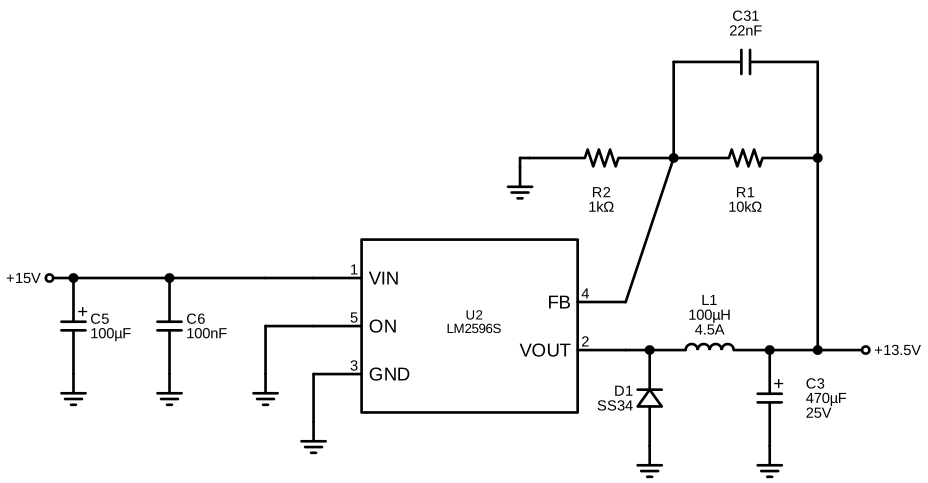
Key points:
Two-stage design: the buck converter drops the voltage at high efficiency, then the linear regulator (U6) provides the low-noise final output.
Capacitor order: C5/C6 (input filter) to
U2 + L1to C3 (buck output filter) toU6to the output capacitors.C3 role: filters switching ripple from the buck converter before it reaches the linear regulator.
Switching node: the junction at OUTPUT pin 2, where L1 and the D1 cathode meet.
D1 freewheeling path: provides the current path while the internal switch is OFF (D1 cathode to the switching node, D1 anode to GND).
The L1 output and the D1 anode are completely separate paths - they do NOT connect to each other. Merging them at layout time shorts the output to ground.
Output voltage:
Vout = 1.23V x (1 + R1/R2)
     = 1.23V x (1 + 10k / 1k)
     = 1.23V x 11
= 13.53V | Ref | Part | Value / note |
|---|---|---|
| L1 | CYA1265-100UH (C19268674) | 100 µH power inductor |
| D1 | SS34 (C8678) | 3A / 40V Schottky catch diode |
| C5 | EFVH035ADA471M10B0 (C22387780) | 470 µF 35V input bulk |
| C6 | CC0805KRX7R9BB104 (C1711) | 100 nF input ceramic, place closest |
| C3 | GVT1E477M0810CNVC (C2983319) | 470 µF 25V buck output filter |
| R1 | 0603WAF1002T5E (C25804) | 10 kΩ upper feedback resistor |
| R2 | 0603WAF1001T5E (C21190) | 1 kΩ lower feedback resistor |
| C31 | CL21B223KBANNNC (C1729) | 22 nF feedforward cap across R1 |
U3: +15V to +7.5V (feeds the +5V rail)
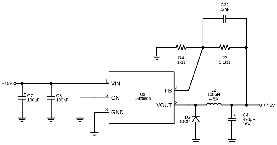
Same buck topology as U2, with a lower output setpoint:
Vout = 1.23V x (1 + R3/R4)
     = 1.23V x (1 + 5.1k / 1k)
     = 1.23V x 6.1
= 7.50V | Ref | Part | Value / note |
|---|---|---|
| L2 | CYA1265-100UH (C19268674) | 100 µH power inductor |
| D2 | SS34 (C8678) | 3A / 40V Schottky catch diode |
| C7 | EFVH035ADA471M10B0 (C22387780) | 470 µF 35V input bulk |
| C8 | CC0805KRX7R9BB104 (C1711) | 100 nF input ceramic |
| C4 | RVT1A471M0607 (C335982) | 470 µF 10V buck output filter |
| R3 | 0603WAF5101T5E (C23186) | 5.1 kΩ upper feedback resistor |
| R4 | 0603WAF1001T5E (C21190) | 1 kΩ lower feedback resistor |
| C32 | CL21B223KBANNNC (C1729) | 22 nF feedforward cap across R3 |
U4: +15V to -13.5V inverting buck-boost (feeds the -12V rail)
U4 is the same LM2596S-ADJ part as U2 and U3, run in an inverting buck-boost configuration. There is no -15V intermediate rail and no LM2586 or SEPIC anywhere in this design; see decision (b) in scripts/ for the evidence trail behind that wording.
In the inverting configuration the IC's own ground pin floats at the negative output. Pin-to-net, from the Board B spec:
| U4 pin | Net | Note |
|---|---|---|
| 1 VIN | +15V -> +13.5V gen | input, shared with the U2/U3 VIN |
| 2 Output (SW) | Net-(D3-K) (L3 + D3) | switch node |
| 3 GND | / | IC ground floats at -Vout |
| 4 FB | Net-(U4-Feedback) (R5 / R6) | sets -13.5V |
| 5 ~ON/OFF | / | enabled (tied to IC ground) |
| 6 TAB | / | tab bootstrapped with the IC ground |
L3 (100 µH) returns to system GND, D3 (SS34) catches to -13.5V OUT, and C11 (470 µF 25V) is the bulk capacitor across -13.5V OUT to GND. C9 (100 µF 50V) and C10 (100 nF) bridge the +15V input to the bootstrapped IC ground, so both see the full 28.5V input-to-output span rather than 15V (fact-lm2596-u4-effective-input). That 28.5V is also what the IC itself sees across its VIN and GND pins, leaving 11.5V to the 40V operating maximum and 16.5V to the 45V absolute maximum.
Output voltage is -13.53V, using the same divider ratio as U2 (R5 10 kΩ, R6 1 kΩ, C33 22 nF feedforward).
Inverting startup draws current-limit inrush from a current-limited source
fact-lm2596-inverting-startup-current records that inverting startup can draw input current up to the switch current limit (roughly 4.5A) for 2 ms or more until the output reaches nominal, and that current-limited input sources may fail to start the converter at all. Board B is fed from exactly such a source - the USB-PD 15V rail through the Board A load switch. The datasheet's own mitigations are a delayed-startup circuit and an enlarged input capacitor. Treat U4 startup as a design item to size and then measure, not as something that will come out right by itself.
The U4 tab is live at -13.5V
Because pin 3, pin 5 and the thermal tab are all bootstrapped to the negative output, the U4 tab copper is not a ground pour. It must be an isolated -13.5V island with full creepage to the surrounding system-ground copper, and it cannot be stitched into the ground plane the way the U2/U3 tabs are.
Feedback resistor selection
The output voltage is set by:
Vout = Vref x (1 + R_upper / R_lower)with Vref = 1.23V (internal reference). Keep R_lower at 1 kΩ, which sets a sensible feedback current, and pick R_upper for the target:
| Target Vout | R_upper | Actual Vout |
|---|---|---|
| 3.3V | 1.7 kΩ | 3.32V |
| 5V | 3.0 kΩ | 4.92V |
| 7.5V | 5.1 kΩ | 7.50V |
| 12V | 8.7 kΩ | 11.93V |
| 13.5V | 10 kΩ | 13.53V |
Use ±1% tolerance parts - the divider ratio lands directly on the output voltage. Separately, the part itself is specified to ±4% maximum over line and load (fact-lm2596-output-tolerance), and the 1.23V reference has its own 1.193V - 1.267V band, so the computed setpoints above are targets rather than guarantees.
Feedback compensation network
All three converters use a Type II compensation network: a feedforward capacitor in parallel with the upper feedback resistor.
Output ──┬─── R_upper ──┬─── R_lower ─── GND
         │              │
         └─── CFF ──────┤
                        │
                       Tap → To FB pin
CFF is C31 (U2), C32 (U3), C33 (U4) - 22 nF ceramic in every position.
In parallel with R_upper: R1 (U2), R3 (U3), R5 (U4).
Why the same 22 nF in all three positions? The compensation capacitor value depends on the switching frequency (150 kHz, identical across the three), the LC filter (100 µH inductor plus a 470 µF-class output capacitor, identical across the three), and the feedback resistor values (which shift DC gain but leave the pole/zero placement close). With the IC, frequency, inductor and output capacitor held constant, one value serves all three circuits.
What the CFF buys:
Better transient response during load steps
Less switching noise coupled onto the feedback line
Suppressed control-loop oscillation
A pole-zero pair for Type II compensation
Reference: LM2596 datasheet, typical application circuit (CFF in Figure 1, page 9).
Inductor selection
Inductance: 100 µH, selectable within roughly 47 µH - 220 µH
Saturation current: at least 1.5x the output current
DCR: as low as practical, it comes straight off efficiency
Selected: CYA1265-100UH, LCSC C19268674, 100 µH. Its 4.5A figure is the datasheet heat rating current (Idc, the DC current for a 40 °C rise at 25 °C ambient), per fact-cya1265-idc-heat-rating - see the CYA1265-100UH record before treating it as a saturation figure.
Diode selection
A Schottky catch diode is required:
Fast enough for the 150 kHz switching edge
Low forward drop, for efficiency
Current rating at or above the output current
Reverse voltage at or above the input voltage (40V or better here)
Selected: SS34, 3A / 40V, LCSC C8678 - see the SS34 record.
Capacitor selection
Input capacitor (VIN to the IC ground reference):
Electrolytic or ceramic
100 µF or more
Voltage rating at least 1.5x the input voltage - and for U4, remember the input capacitors bridge +15V to -13.5V, so rate them for the full 28.5V span
Output capacitor (VOUT to GND):
Low-ESR electrolytic
220 µF - 1000 µF (470 µF here)
ESR 0.5 Ω or less, for ripple
Voltage rating at least 1.5x the output voltage
PCB layout guidelines
Switching loop: minimize the area of the VIN - IC - L - D - Cout loop.
Ground plane: keep a continuous, wide ground plane under the U2/U3 stages.
Thermal relief: connect the U2/U3 TO-263 tabs directly to the ground plane - no thermal-relief spokes. The U4 tab is a -13.5V island instead (see the warning above).
FB trace: keep the feedback trace short and away from the switching node.
Vias: place multiple thermal vias under each tab.
Recommended trace widths:
VIN, VOUT: 2 mm or wider (3A capability)
GND: as wide as possible, plane preferred
FB: 0.2 mm - 0.3 mm, thin and short
Efficiency
Factors, in the order they usually matter:
Inductor DCR - lower is better
Diode forward drop - lower is better, hence Schottky
Output capacitor ESR - lower is better
Input-to-output voltage difference - a smaller difference is more efficient
Working estimates for this design (not measured):
U2 (15V to 13.5V): ~88%
U3 (15V to 7.5V): ~85%
U4 (+15V to -13.5V inverting): ~88%
ON/OFF pin wiring
The ON/OFF pin (pin 5) is referenced to pin 3, the IC ground, not to system ground. That distinction is what makes the buck and the inverting buck-boost cases different.
Regular buck (U2, U3)
Pin 5 is tied to system GND (0V), or left floating.
U2, U3 (buck converters):
Pin 5 (ON/OFF) ──→ System GND (0V)
Pin 3 (IC GND)  ──→ System GND (0V)
The IC ground pin is at 0V, so the thresholds referenced to it are also the system thresholds. Per fact-lm2596-onoff-thresholds the typical threshold is 1.3V, with the regulator guaranteed ON at 0.6V or below and guaranteed OFF at 2V or above. Tying to system GND is LOW, which is enabled.
Inverting buck-boost (U4)
Pin 5 is tied to IC ground, which sits at -13.5V, or left floating.
U4 (inverting buck-boost):
Pin 5 (ON/OFF) ──→ IC GND (-13.5V) [same net as pin 3]
Pin 3 (IC GND)  ──→ -13.5V output (bootstrapped)
The critical difference: the IC ground pin is at -13.5V, not at system ground. The thresholds, being referenced to that pin, all shift down by 13.5V: guaranteed ON at -12.9V or below, typical threshold at -12.2V, guaranteed OFF at -11.5V or above, all in system terms. Connecting pin 5 to system GND would put it 13.5V above IC ground - that is a shutdown command, not an enable. Tie it to IC ground, or leave it floating.
| Topology | IC GND sits at | ON pin connection | Enabled | Disabled |
|---|---|---|---|---|
| U2, U3 (buck) | System GND (0V) | System GND or float | <= 0.6V (system ref) | >= 2V (system ref) |
| U4 (inverting) | -13.5V output | IC GND or float | <= -12.9V (system ref) | >= -11.5V (system ref) |
Guaranteed limits from fact-lm2596-onoff-thresholds; the typical threshold sits at 1.3V above the IC ground pin, so -12.2V in system terms for U4.
Why this matters
For always-on operation (what this project does):
U2, U3: tie the ON pin to system GND. Explicit beats floating, for noise immunity.
U4: tie the ON pin to IC ground (pin 3, at -13.5V).
For shutdown control (not used here):
U2, U3: simple - pull the pin to 2V or above, system-ground referenced.
U4: needs an optocoupler or level shifter, because the control signal has to be referenced to a rail that moves. See TI application note SNVA722B.
Internal pull-down
The LM2596S has an internal pull-down on the ON/OFF pin. It pulls toward IC ground, wherever that happens to be, so a floating pin reads LOW relative to IC ground and the part is enabled in both topologies. Connect the pin explicitly anyway - relying on the internal pull-down gives up noise immunity for nothing.
Thermal
fact-lm2596-thermal records the TO-263 thermal resistance as a function of tab copper area, all with 1 oz copper:
| Tab copper area | thetaJA |
|---|---|
| 0.5 in² | 50 °C/W |
| 2.5 in² | 30 °C/W |
| 3 in² plus roughly 16 in² backside | 20 °C/W |
thetaJC is 2 °C/W; the operating junction range is -40 °C to +125 °C, with a 150 °C absolute maximum. The fact carries a NEEDS BENCH verdict: Board B has no layout yet, so neither the actual copper area nor the actual dissipation is settled. Size the tab pour against the table above once the layout exists, then confirm on the bench - do not quote a junction temperature from an assumed copper area.
Related
Linear Regulator PCB Layout and Thermal Design - the LDO stage these converters feed