KiCad Project Workflow
Complete workflow for creating a PCB design in KiCad, from schematic to manufacturing files.
This page's Stage 1-2 hand-drawing workflow is for the legacy root project only
Board A and Board B (boards/board-a/, boards/board-b/) are not drawn by hand in KiCad's Schematic Editor — see Spec-driven schematic generationdirectly below. The rest of this page (Stage 1: Symbol Management through Stage 2: Schematic Creation) describes the manual workflow used for the legacy root project(zudo-pd.kicad_pro / zudo-pd.kicad_sch and its sub-sheets) — the as-built v4 reference, which stays hand-edited. Stage 3 onward (footprint assignment, PCB layout, manufacturing outputs, JLCPCB ordering) applies once a board has a schematic, regardless of whether that schematic was hand-drawn or generated, and is not yet exercised for Board A/B since neither has a PCB layout.
Spec-driven schematic generation (boards/board-a / boards/board-b)
Board A and Board B schematics are generated from a Python spec module by the schgen toolchain — the spec module (scripts/ / board_b_spec.py) is the source of truth; the .kicad_sch file it produces is a build artifact. Never hand-edit boards/ or boards/ directly — edit the spec module and regenerate.
1. Edit the spec module
Each spec module defines three tables: COMPONENTS (ref → symbol/value/LCSC/footprint/ DNP/position), NETS (net name → list of Ref.Pin tokens), and NO_CONNECT (pins explicitly left unconnected). Add/move a component, change a net, or add a no-connect by editing these tables — not the generated schematic.
2. Regenerate the schematic
python3 scripts/schgen/gen_schematic.py board_a_spec # or board_b_specThe argument is an importable module name (board_a_spec), not a file path — there is no --help. This rewrites boards/<board>/<board>.kicad_sch in place. No KiCad install is required for this step; gen_schematic.py only depends on the dependency-free sexp.py s-expression parser.
3. Verify against a real netlist export (requires local KiCad)
scripts/schgen/verify.sh board-a # or board-bThis runs kicad-cli sch export netlist on the regenerated schematic, then diffs the result against the spec module's NETS/NO_CONNECT tables via verify_netlist.py, printing PASS/FAIL. It degrades gracefully (prints SKIPPED, exits 0) when kicad-cli is not on PATH — this is a local-only check; CI has no KiCad install.
4. Check the decision lock and the connectivity baseline (offline, no KiCad needed)
python3 scripts/schgen/check_decisions.py    # validates scripts/schgen/decisions.json

# diff each spec's NETS against its locked baseline (with the allow-list of
# intentional deltas) — the same invocations CI runs:
python3 scripts/schgen/check_baseline.py scripts/schgen/board_a_spec.py scripts/schgen/baselines/board-a.json --allow scripts/schgen/baselines/board-a-allowed-deltas.json
python3 scripts/schgen/check_baseline.py scripts/schgen/board_b_spec.py scripts/schgen/baselines/board-b.json --allow scripts/schgen/baselines/board-b-allow.json
decisions.json is the machine-consumable record of every wave-6 component-level decision (part swaps, provisions, dispositions) the spec modules must implement, with rationale and fact-ID evidence per decision — see Spec-Architecture Review for the full findings these decisions resolve. check_baseline.py diffs a spec module's NETS table against its recorded connectivity baseline (scripts/ / board-b.json) plus an explicit allow-list of intentional deltas, so an accidental net change during a spec edit fails loudly instead of silently drifting.
5. Open in KiCad and commit together
Open the regenerated schematic in KiCad's Eeschema at least once (ERC, visual sanity) before committing. Commit the spec module and the regenerated .kicad_sch together — never one without the other, so a regen-from-clean leaves boards/ unchanged (the regen-idempotency invariant CI enforces today on every PR — see scripts/, "What CI checks").
Smoke-testing the generator itself
After touching schgen_core.py or sexp.py (not a spec module), sanity-check the generator with:
bash scripts/schgen/run_smoke_test.shThis regenerates a throwaway 3-component test spec into a temp directory (never touches the repo tree) and asserts the emitted net labels match the spec — no pip installs, no KiCad, stock python3 only.
Full reference: scripts/.
Legacy manual workflow (root-level KiCad project only)
The stages below describe hand-drawing the root project's schematic and PCB (zudo-pd.kicad_pro and its sub-sheets) directly in KiCad's GUI. This is how the v1–v4 as-built boards were designed; it does not apply to boards/board-a/boards/board-b.
Prerequisites
CRITICAL: Before starting, ensure your KiCad project files are located at the repository root:
zudo-pd/          ← Repository root
├── zudo-pd.kicad_pro       ← Project file must be here
├── zudo-pd.kicad_sch       ← Schematic file
├── zudo-pd.kicad_pcb       ← PCB file (created later)
└── footprints/             ← Footprint library
    └── kicad/
        └── zudo-power.pretty/
The ${KIPRJMOD} variable in KiCad points to the directory containing the .kicad_pro file. If your project is in a subdirectory (like kicad/ or pcb/), relative paths to footprints and libraries won't resolve correctly.
Overview
KiCad uses a modular workflow where you work with different editors in sequence:
Symbol Editor - Create/import schematic symbols
Schematic Editor - Draw circuit diagrams
Footprint Editor - Create/import PCB footprints
PCB Editor - Layout the physical board
Manufacturing Output - Generate Gerber files
Stage 1: Symbol Management
1.1 Check Existing Libraries
Before creating custom symbols, check if they already exist in KiCad's standard libraries:
Common libraries for this project:
Device- Resistors, capacitors, inductors, diodes, LEDsRegulator_Linear- LM78xx, LM79xx seriesRegulator_Switching- LM2596, buck/boost convertersConnector- USB connectors, power jacks, headerspower- GND, VCC, voltage symbols
To check:
Open Symbol Editor
File → Add Library... → Browse standard KiCad libraries
Search for your part number or category
1.2 Import Symbols from Standard Libraries
For parts already in KiCad libraries:
Open Schematic Editor
Press
A(Add Symbol)Search by part name (e.g., "LM7812", "USB_C_Receptacle")
Browse by library category if unsure
1.3 Create Custom Symbols
For parts NOT in standard libraries (like STUSB4500, specialized ICs):
Method 1: Import from EasyEDA/LCSC
Use easyeda2kicad.py to download both symbols and footprints:
# Download symbol + footprint for STUSB4500 (LCSC ID: C2678061)
easyeda2kicad --lcsc_id C2678061 --symbol --footprint

# Files saved to:
# ~/Documents/Kicad/easyeda2kicad/easyeda2kicad.pretty/  (footprints)
# ~/Documents/Kicad/easyeda2kicad/easyeda2kicad.kicad_sym (symbols)
Method 2: Manual Creation
Open Symbol Editor
File → New Library... → Create project-specific library (e.g.,
zudo-power.kicad_sym)Create New Symbol
Define:
Pin numbers and names (from datasheet)
Pin electrical types (input, output, power, passive)
Symbol shape (rectangle, specialized)
Reference designator (U, R, C, J, etc.)
Best practices:
Match datasheet pin numbering exactly
Use descriptive pin names (VIN, VOUT, FB, EN, etc.)
Set correct electrical types for ERC (Electrical Rule Check)
Add datasheet link in symbol properties
Stage 2: Schematic Creation
2.1 Create New Schematic
Open Schematic Editor (
zudo-pd.kicad_sch)Set up page properties:
Title: "USB-PD Modular Synth Power Supply"
Revision: v1.0
Date: (automatic)
Company/Organization (optional)
2.2 Place Symbols
Press
Ato add symbolsSearch and place all components
Use logical groupings:
USB-PD input stage (left side)
DC-DC converters (center)
Linear regulators (right)
Output connectors (far right)
Recommended layout flow:
Left to Right = Signal Flow
USB-C Input → DC-DC Conversion → Linear Regulation → Outputs
2.3 Wire Connections
Press
Wto start wiringClick start point → Click end point
Use labels for:
Power nets:
+15V,+13.5V,+7.5V,-13.5V,+12V,+5V,-12VGround:
GND(use power symbol)Signal names:
PG(Power Good),EN(Enable),FB(Feedback)
Best practices:
Use net labels instead of long wires across the page
Group related components close together
Keep power flow left-to-right, top-to-bottom
Add
No Connectflags (X) to unused pins
2.4 Add Power Symbols
Press
Pto add power symbolsAdd for each voltage rail:
+12V,+5V,-12V(outputs)+15V,+13.5V,-13.5V(intermediate)GND(ground reference)
2.5 Add Values and References
For each component:
Select component
Press
Eto edit propertiesSet:
Reference (auto-numbered: U1, R1, C1, etc.)
Value (10µF, 5.1kΩ, LM7812, etc.)
Footprint (assigned in next step)
Datasheet URL (optional but recommended)
2.6 Annotate Schematic
Auto-number all reference designators:
Tools → Annotate Schematic
Select "Use entire schematic" (for multi-sheet projects)
Click "Annotate"
Result: R?, C?, U? become R1, R2, C1, C2, U1, U2, etc.
2.7 Electrical Rules Check (ERC)
Before proceeding to PCB:
Inspect → Electrical Rules Checker
Run ERC
Fix all errors:
Unconnected pins
Power pins not driven
Conflicting outputs
Missing power connections
Stage 3: Footprint Assignment
3.1 Import Footprints
For JLCPCB-compatible parts:
See KiCad Parts Download Guide for detailed instructions.
Quick workflow:
# Download footprint by LCSC ID
easyeda2kicad --lcsc_id C970725 --footprint

# Copy to project directory
cp ~/Documents/Kicad/easyeda2kicad/easyeda2kicad.pretty/*.kicad_mod ./footprints/kicad/
3.1a Add Footprint Library to KiCad
IMPORTANT: Before adding the footprint library, ensure your KiCad project (.kicad_pro file) is located in the repository root directory. The ${KIPRJMOD} variable points to the project file location, so if your project is in a subdirectory (like kicad/), the relative paths won't resolve correctly.
Project structure:
zudo-pd/          ← Repository root
├── zudo-pd.kicad_pro       ← KiCad project file should be here
├── zudo-pd.kicad_sch       ← Schematic file
├── zudo-pd.kicad_pcb       ← PCB file
└── footprints/
    └── kicad/
        └── zudo-power.pretty/   ← Footprint library
            ├── C0603.kicad_mod
            ├── C0805.kicad_mod
            └── ... (37 footprints)
Steps to add footprint library:
Open Preferences → Manage Footprint Libraries
From main KiCad window (NOT Symbol Editor)
Or from PCB Editor: Preferences → Manage Footprint Libraries
Click "Project Specific Libraries" tab (at bottom)
Add new library:
Click folder icon (➕) to add library
Set values:
Nickname:
zudo-pd(or any name you prefer)Library Path:
${KIPRJMOD}/footprints/ kicad/ zudo- power. pretty Library Format:
KiCadOptions: (leave blank)
Click OK
Example configuration:
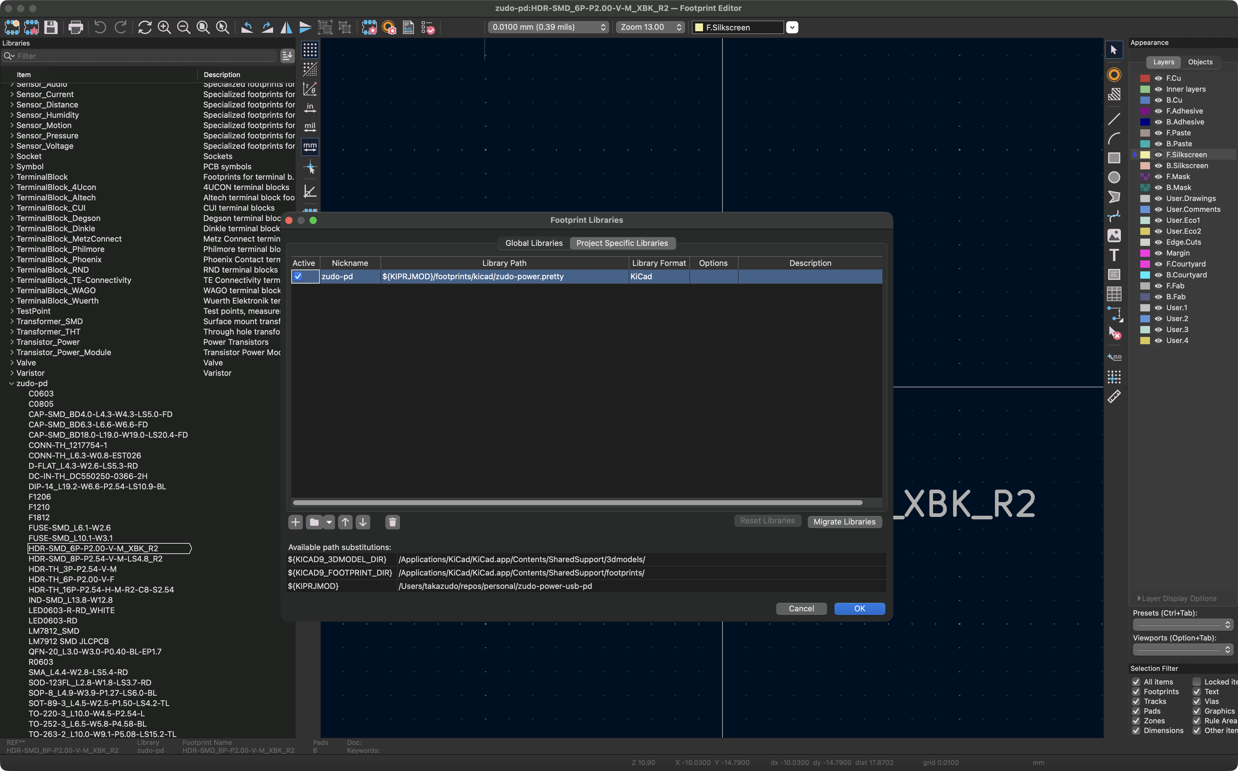
The dialog should show:
Library nickname:
zudo-pdLibrary path:
${KIPRJMOD}/footprints/ kicad/ zudo- power. pretty At the bottom, "Available path substitutions" shows the resolved path
Verify the library loaded:
Open Footprint Editor (from main KiCad window)
Check left panel - you should see
zudo-pdlibraryClick on it to expand and browse 37 footprints
You should see footprints like:
C0603,C0805(capacitors)TO-252-3,TO-263-2(IC packages)SOP-8,SSOP-10(IC packages)Component-specific footprints
Troubleshooting:
Library appears empty: Verify the path points to
zudo-power.prettydirectory (not.prettyor other directories)Path not found: Check that
${KIPRJMOD}resolves correctly by looking at "Available path substitutions" at bottom of dialogWrong symbols showing: You opened Symbol Libraries instead of Footprint Libraries - close and reopen the correct dialog
3.2 Assign Footprints to Symbols
In Schematic Editor: Tools → Assign Footprints
For each component, select appropriate footprint:
Resistors/Capacitors:
0805,1206(SMD sizes)ICs: Match package type from datasheet (SOIC-8, SOT-23-6, etc.)
Connectors: Match mechanical dimensions exactly
Large components: Verify pad sizes for current rating
Example assignments:
LM7812 →
TO-263-2(D2PAK-2, fitted part is L7812CD2T-TR)LM2596S →
TO-263-5(D2PAK)STUSB4500 →
QFN-24(from LCSC)10µF capacitor →
C_0805_2012Metric5.1kΩ resistor →
R_0805_2012Metric
3.3 Verify Footprint Assignments
Check that ALL components have footprints assigned (no "No Footprint" entries)
Verify footprint sizes match your requirements:
Small passives: 0805 or 1206 (easy hand soldering)
ICs: Match JLCPCB assembly capabilities
Connectors: Match mechanical specs exactly
Stage 4: PCB Layout
4.1 Generate Netlist and Import to PCB
In Schematic Editor: Tools → Update PCB from Schematic (F8)
Click "Update PCB"
PCB Editor opens with all components loaded
First import: Components appear in a cluster, ready to be positioned
4.2 Set Board Dimensions
Select Edge.Cuts layer
Draw board outline:
Press
Ctrl+Shift+Pfor polygon toolDraw rectangle or custom shape
Recommended: Start with 100mm × 80mm for this project
4.3 Place Components
Strategic placement:
Input stage (left):
USB-C connector on board edge
STUSB4500 near connector
Input capacitors near STUSB4500
DC-DC stage (center):
LM2596S converters in row
Inductors next to each converter
Output capacitors after inductors
Linear regulators (right of center):
LM7812, LM7805, LM7912 in row
Input/output capacitors adjacent
Output connectors (right edge):
Power headers on board edge
Fuses before output
TVS diodes near output
Best practices:
Keep signal paths short (especially high-current paths)
Place decoupling capacitors close to IC power pins
Orient components for logical layout
Leave space for heat dissipation (regulators, DC-DC)
Group by function, not just by type
4.4 Route Traces
Layer strategy:
F.Cu (Top layer): Power traces, signal routing
B.Cu (Bottom layer): Ground plane + additional routing
Trace widths (for 1oz copper):
Power traces (1A+): 0.5mm minimum, 1.0mm recommended
Signal traces: 0.25mm minimum, 0.3mm recommended
Ground/return: Wide as possible, or use ground plane
Routing order:
Route power traces first (+15V, +12V, +5V, -12V)
Route critical signals (feedback, enable pins)
Route remaining connections
Add ground plane on bottom layer (Fill Zone)
Tools:
Press
Xto start routingPress
Vto add via (switch layers)Press
Dto drag component while maintaining connections
4.5 Add Ground Plane
Select B.Cu layer
Press
Ctrl+Shift+Zto add filled zoneDraw zone around entire board
Set net:
GNDPress
Bto rebuild all zones
4.6 Design Rule Check (DRC)
Before manufacturing:
Inspect → Design Rules Checker
Run DRC
Fix all errors:
Trace clearance violations
Unconnected nets
Board outline issues
Silkscreen over pads
Stage 5: Manufacturing Output
5.1 Generate Gerber Files
File → Fabrication Outputs → Gerbers (.gbr)
Settings:
Include layers: F.Cu, B.Cu, F.Mask, B.Mask, F.Silkscreen, B.Silkscreen, Edge.Cuts
Coordinate format: 4.6, unit mm
Check "Use Protel filename extensions"
Click "Plot"
5.2 Generate Drill Files
File → Fabrication Outputs → Drill Files (.drl)
Settings:
Drill units: Millimeters
Drill map: PostScript or PDF (for verification)
Click "Generate Drill File"
5.3 Generate BOM (Bill of Materials)
In Schematic Editor: File → Fabrication Outputs → BOM
Use built-in generator or:
Export to CSV
Use external tool (KiBoM, InteractiveHtmlBom)
For JLCPCB assembly:
Must include: Reference, Value, Footprint, LCSC Part Number
Export as CSV format
Match JLCPCB template exactly
5.4 Generate Pick-and-Place File
For SMT assembly:
File → Fabrication Outputs → Component Placement (.pos)
Format: CSV
Units: Millimeters
Includes: Reference, X, Y, Rotation, Layer
5.5 Verify with Gerber Viewer
Open GerbView (included with KiCad)
Load all Gerber files + drill file
Check:
Board outline correct
All pads visible
Silkscreen readable (not over pads)
Drill holes aligned with pads
Layers aligned correctly
Stage 6: Order from JLCPCB
6.1 Prepare Files
Create ZIP archive with:
All Gerber files (.gbr)
Drill file (.drl)
BOM (CSV format, JLCPCB template)
Pick-and-place file (CSV format)
# Example ZIP structure
gerbers.zip
├── F_Cu.gbr
├── B_Cu.gbr
├── F_Mask.gbr
├── B_Mask.gbr
├── F_Silkscreen.gbr
├── B_Silkscreen.gbr
├── Edge_Cuts.gbr
└── drill.drl

bom_jlcpcb.csv
cpl_jlcpcb.csv
6.2 Upload and Configure
Go to jlcpcb.com
Upload gerbers.zip
Configure:
PCB quantity: 5 (minimum)
PCB thickness: 1.6mm (standard)
Surface finish: HASL (lead-free) or ENIG (better quality)
Copper weight: 1oz (standard for <3A)
Add SMT assembly service (optional):
Upload BOM + CPL
Review component placement
Check part availability/substitutions
Workflow Summary
1. Symbol Editor
   ↓
2. Schematic Editor → [ERC Pass] → Assign Footprints
   ↓
3. Update PCB from Schematic
   ↓
4. PCB Editor → Place Components → Route → [DRC Pass]
   ↓
5. Generate Outputs (Gerber, Drill, BOM, CPL)
   ↓
6. Verify in GerbView
   ↓
7. Order from JLCPCB
Troubleshooting
Common Issues
Problem: Symbol not found when placing component
Solution: Add library containing the symbol (Preferences → Manage Symbol Libraries)
Problem: Footprint assignment shows "No Footprint"
Solution: Add footprint library (Preferences → Manage Footprint Libraries)
Problem: DRC shows "unconnected nets"
Solution: Check for missing wires in schematic, or use "No Connect" flags
Problem: Gerber viewer shows misaligned layers
Solution: Check drill origin settings, regenerate Gerbers with correct settings
Problem: JLCPCB BOM upload fails
Solution: Verify CSV format matches template, check for special characters
Next Steps
After completing the KiCad workflow:
Documentation:
Update parts list with LCSC IDs
Document connectivity using the net-table convention
Testing plan:
Order PCBs without assembly first
Verify board dimensions and mounting holes
Check component footprints with actual parts
Then order with assembly
Version control:
Commit KiCad project files (.kicad_pro, .kicad_sch, .kicad_pcb)
Commit Gerber outputs for reference
Tag checkpoints per the project's X.Y.Z versioning scheme (see
.) — not free-form release tags like v1.0/v1.1. / inbox/ versioning. md
References
scripts/— full spec-driven regen/verify workflow referenceschgen/ README. md Spec-Architecture Review and
scripts/— the evidence review and locked decision set the spec modules implementschgen/ decisions. json