KiCad Project Workflow
Complete workflow for creating a PCB design in KiCad, from schematic to manufacturing files.
Prerequisites
CRITICAL: Before starting, ensure your KiCad project files are located at the repository root:
zudo-The ${KIPRJMOD} variable in KiCad points to the directory containing the .kicad_pro file. If your project is in a subdirectory (like kicad/ or pcb/), relative paths to footprints and libraries won't resolve correctly.
Overview
KiCad uses a modular workflow where you work with different editors in sequence:
Symbol Editor - Create/import schematic symbols
Schematic Editor - Draw circuit diagrams
Footprint Editor - Create/import PCB footprints
PCB Editor - Layout the physical board
Manufacturing Output - Generate Gerber files
Stage 1: Symbol Management
1.1 Check Existing Libraries
Before creating custom symbols, check if they already exist in KiCad's standard libraries:
Common libraries for this project:
Device- Resistors, capacitors, inductors, diodes, LEDsRegulator_Linear- LM78xx, LM79xx seriesRegulator_Switching- LM2596, buck/boost convertersConnector- USB connectors, power jacks, headerspower- GND, VCC, voltage symbols
To check:
Open Symbol Editor
File → Add Library... → Browse standard KiCad libraries
Search for your part number or category
1.2 Import Symbols from Standard Libraries
For parts already in KiCad libraries:
Open Schematic Editor
Press
A(Add Symbol)Search by part name (e.g., "LM7812", "USB_C_Receptacle")
Browse by library category if unsure
1.3 Create Custom Symbols
For parts NOT in standard libraries (like STUSB4500, specialized ICs):
Method 1: Import from EasyEDA/LCSC
Use easyeda2kicad.py to download both symbols and footprints:
# Download symbol + footprint for STUSB4500 (LCSC ID: C2678061)
easyeda2kicad --lcsc_id C2678061 --symbol --footprint

# Files saved to:
# ~/Documents/Kicad/easyeda2kicad/easyeda2kicad.pretty/  (footprints)
# ~/Documents/Kicad/easyeda2kicad/easyeda2kicad.kicad_sym (symbols)
Method 2: Manual Creation
Open Symbol Editor
File → New Library... → Create project-specific library (e.g.,
zudo-power.kicad_sym)Create New Symbol
Define:
Pin numbers and names (from datasheet)
Pin electrical types (input, output, power, passive)
Symbol shape (rectangle, specialized)
Reference designator (U, R, C, J, etc.)
Best practices:
Match datasheet pin numbering exactly
Use descriptive pin names (VIN, VOUT, FB, EN, etc.)
Set correct electrical types for ERC (Electrical Rule Check)
Add datasheet link in symbol properties
Stage 2: Schematic Creation
2.1 Create New Schematic
Open Schematic Editor (
zudo-pd.kicad_sch)Set up page properties:
Title: "USB-PD Modular Synth Power Supply"
Revision: v1.0
Date: (automatic)
Company/Organization (optional)
2.2 Place Symbols
Press
Ato add symbolsSearch and place all components
Use logical groupings:
USB-PD input stage (left side)
DC-DC converters (center)
Linear regulators (right)
Output connectors (far right)
Recommended layout flow:
Left to Right = Signal Flow
USB-C Input → DC-DC Conversion → Linear Regulation → Outputs
2.3 Wire Connections
Press
Wto start wiringClick start point → Click end point
Use labels for:
Power nets:
+15V,+13.5V,+12V,+5V,-12V,-15VGround:
GND(use power symbol)Signal names:
PG(Power Good),EN(Enable),FB(Feedback)
Best practices:
Use net labels instead of long wires across the page
Group related components close together
Keep power flow left-to-right, top-to-bottom
Add
No Connectflags (X) to unused pins
2.4 Add Power Symbols
Press
Pto add power symbolsAdd for each voltage rail:
+12V,+5V,-12V(outputs)+15V,+13.5V,-13.5V(intermediate)GND(ground reference)
2.5 Add Values and References
For each component:
Select component
Press
Eto edit propertiesSet:
Reference (auto-numbered: U1, R1, C1, etc.)
Value (10µF, 5.1kΩ, LM7812, etc.)
Footprint (assigned in next step)
Datasheet URL (optional but recommended)
2.6 Annotate Schematic
Auto-number all reference designators:
Tools → Annotate Schematic
Select "Use entire schematic" (for multi-sheet projects)
Click "Annotate"
Result: R?, C?, U? become R1, R2, C1, C2, U1, U2, etc.
2.7 Electrical Rules Check (ERC)
Before proceeding to PCB:
Inspect → Electrical Rules Checker
Run ERC
Fix all errors:
Unconnected pins
Power pins not driven
Conflicting outputs
Missing power connections
Stage 3: Footprint Assignment
3.1 Import Footprints
For JLCPCB-compatible parts:
See KiCad Parts Download Guide for detailed instructions.
Quick workflow:
# Download footprint by LCSC ID
easyeda2kicad --lcsc_id C970725 --footprint

# Copy to project directory
cp ~/Documents/Kicad/easyeda2kicad/easyeda2kicad.pretty/*.kicad_mod ./footprints/kicad/
3.1a Add Footprint Library to KiCad
IMPORTANT: Before adding the footprint library, ensure your KiCad project (.kicad_pro file) is located in the repository root directory. The ${KIPRJMOD} variable points to the project file location, so if your project is in a subdirectory (like kicad/), the relative paths won't resolve correctly.
Project structure:
zudo-Steps to add footprint library:
Open Preferences → Manage Footprint Libraries
From main KiCad window (NOT Symbol Editor)
Or from PCB Editor: Preferences → Manage Footprint Libraries
Click "Project Specific Libraries" tab (at bottom)
Add new library:
Click folder icon (➕) to add library
Set values:
Nickname:
zudo-pd(or any name you prefer)Library Path:
${KIPRJMOD}/footprints/ kicad/ zudo- power. pretty Library Format:
KiCadOptions: (leave blank)
Click OK
Example configuration:
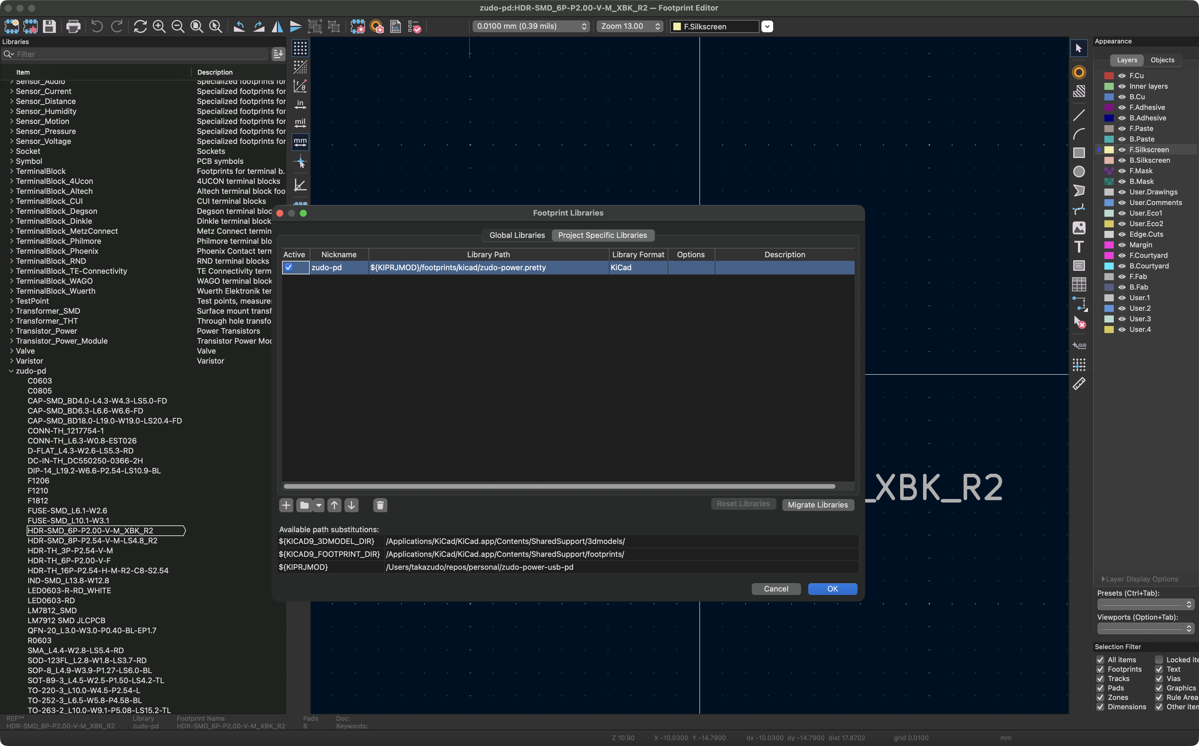
The dialog should show:
Library nickname:
zudo-pdLibrary path:
${KIPRJMOD}/footprints/ kicad/ zudo- power. pretty At the bottom, "Available path substitutions" shows the resolved path
Verify the library loaded:
Open Footprint Editor (from main KiCad window)
Check left panel - you should see
zudo-pdlibraryClick on it to expand and browse 37 footprints
You should see footprints like:
C0603,C0805(capacitors)TO-252-3,TO-263-2(IC packages)SOP-8,SSOP-10(IC packages)Component-specific footprints
Troubleshooting:
Library appears empty: Verify the path points to
zudo-power.prettydirectory (not.prettyor other directories)Path not found: Check that
${KIPRJMOD}resolves correctly by looking at "Available path substitutions" at bottom of dialogWrong symbols showing: You opened Symbol Libraries instead of Footprint Libraries - close and reopen the correct dialog
3.2 Assign Footprints to Symbols
In Schematic Editor: Tools → Assign Footprints
For each component, select appropriate footprint:
Resistors/Capacitors:
0805,1206(SMD sizes)ICs: Match package type from datasheet (SOIC-8, SOT-23-6, etc.)
Connectors: Match mechanical dimensions exactly
Large components: Verify pad sizes for current rating
Example assignments:
LM7812 →
TO-252-2(DPAK)LM2596S →
TO-263-5(D2PAK)STUSB4500 →
QFN-24(from LCSC)10µF capacitor →
C_0805_2012Metric5.1kΩ resistor →
R_0805_2012Metric
3.3 Verify Footprint Assignments
Check that ALL components have footprints assigned (no "No Footprint" entries)
Verify footprint sizes match your requirements:
Small passives: 0805 or 1206 (easy hand soldering)
ICs: Match JLCPCB assembly capabilities
Connectors: Match mechanical specs exactly
Stage 4: PCB Layout
4.1 Generate Netlist and Import to PCB
In Schematic Editor: Tools → Update PCB from Schematic (F8)
Click "Update PCB"
PCB Editor opens with all components loaded
First import: Components appear in a cluster, ready to be positioned
4.2 Set Board Dimensions
Select Edge.Cuts layer
Draw board outline:
Press
Ctrl+Shift+Pfor polygon toolDraw rectangle or custom shape
Recommended: Start with 100mm × 80mm for this project
4.3 Place Components
Strategic placement:
Input stage (left):
USB-C connector on board edge
CH224Q near connector
Input capacitors near CH224Q
DC-DC stage (center):
LM2596S converters in row
Inductors next to each converter
Output capacitors after inductors
Linear regulators (right of center):
LM7812, LM7805, LM7912 in row
Input/output capacitors adjacent
Output connectors (right edge):
Power headers on board edge
Fuses before output
TVS diodes near output
Best practices:
Keep signal paths short (especially high-current paths)
Place decoupling capacitors close to IC power pins
Orient components for logical layout
Leave space for heat dissipation (regulators, DC-DC)
Group by function, not just by type
4.4 Route Traces
Layer strategy:
F.Cu (Top layer): Power traces, signal routing
B.Cu (Bottom layer): Ground plane + additional routing
Trace widths (for 1oz copper):
Power traces (1A+): 0.5mm minimum, 1.0mm recommended
Signal traces: 0.25mm minimum, 0.3mm recommended
Ground/return: Wide as possible, or use ground plane
Routing order:
Route power traces first (+15V, +12V, +5V, -12V)
Route critical signals (feedback, enable pins)
Route remaining connections
Add ground plane on bottom layer (Fill Zone)
Tools:
Press
Xto start routingPress
Vto add via (switch layers)Press
Dto drag component while maintaining connections
4.5 Add Ground Plane
Select B.Cu layer
Press
Ctrl+Shift+Zto add filled zoneDraw zone around entire board
Set net:
GNDPress
Bto rebuild all zones
4.6 Design Rule Check (DRC)
Before manufacturing:
Inspect → Design Rules Checker
Run DRC
Fix all errors:
Trace clearance violations
Unconnected nets
Board outline issues
Silkscreen over pads
Stage 5: Manufacturing Output
5.1 Generate Gerber Files
File → Fabrication Outputs → Gerbers (.gbr)
Settings:
Include layers: F.Cu, B.Cu, F.Mask, B.Mask, F.Silkscreen, B.Silkscreen, Edge.Cuts
Coordinate format: 4.6, unit mm
Check "Use Protel filename extensions"
Click "Plot"
5.2 Generate Drill Files
File → Fabrication Outputs → Drill Files (.drl)
Settings:
Drill units: Millimeters
Drill map: PostScript or PDF (for verification)
Click "Generate Drill File"
5.3 Generate BOM (Bill of Materials)
In Schematic Editor: File → Fabrication Outputs → BOM
Use built-in generator or:
Export to CSV
Use external tool (KiBoM, InteractiveHtmlBom)
For JLCPCB assembly:
Must include: Reference, Value, Footprint, LCSC Part Number
Export as CSV format
Match JLCPCB template exactly
5.4 Generate Pick-and-Place File
For SMT assembly:
File → Fabrication Outputs → Component Placement (.pos)
Format: CSV
Units: Millimeters
Includes: Reference, X, Y, Rotation, Layer
5.5 Verify with Gerber Viewer
Open GerbView (included with KiCad)
Load all Gerber files + drill file
Check:
Board outline correct
All pads visible
Silkscreen readable (not over pads)
Drill holes aligned with pads
Layers aligned correctly
Stage 6: Order from JLCPCB
6.1 Prepare Files
Create ZIP archive with:
All Gerber files (.gbr)
Drill file (.drl)
BOM (CSV format, JLCPCB template)
Pick-and-place file (CSV format)
# Example ZIP structure
gerbers.zip
├── F_Cu.gbr
├── B_Cu.gbr
├── F_Mask.gbr
├── B_Mask.gbr
├── F_Silkscreen.gbr
├── B_Silkscreen.gbr
├── Edge_Cuts.gbr
└── drill.drl

bom_jlcpcb.csv
cpl_jlcpcb.csv
6.2 Upload and Configure
Go to jlcpcb.com
Upload gerbers.zip
Configure:
PCB quantity: 5 (minimum)
PCB thickness: 1.6mm (standard)
Surface finish: HASL (lead-free) or ENIG (better quality)
Copper weight: 1oz (standard for <3A)
Add SMT assembly service (optional):
Upload BOM + CPL
Review component placement
Check part availability/substitutions
Workflow Summary
1. Symbol Editor
   ↓
2. Schematic Editor → [ERC Pass] → Assign Footprints
   ↓
3. Update PCB from Schematic
   ↓
4. PCB Editor → Place Components → Route → [DRC Pass]
   ↓
5. Generate Outputs (Gerber, Drill, BOM, CPL)
   ↓
6. Verify in GerbView
   ↓
7. Order from JLCPCB
Troubleshooting
Common Issues
Problem: Symbol not found when placing component
Solution: Add library containing the symbol (Preferences → Manage Symbol Libraries)
Problem: Footprint assignment shows "No Footprint"
Solution: Add footprint library (Preferences → Manage Footprint Libraries)
Problem: DRC shows "unconnected nets"
Solution: Check for missing wires in schematic, or use "No Connect" flags
Problem: Gerber viewer shows misaligned layers
Solution: Check drill origin settings, regenerate Gerbers with correct settings
Problem: JLCPCB BOM upload fails
Solution: Verify CSV format matches template, check for special characters
Next Steps
After completing the KiCad workflow:
Documentation:
Export circuit diagram as SVG (see Create Circuit SVG Files)
Export footprint previews (see Create Footprint SVG Files)
Update parts list with LCSC IDs
Testing plan:
Order PCBs without assembly first
Verify board dimensions and mounting holes
Check component footprints with actual parts
Then order with assembly
Version control:
Commit KiCad project files (.kicad_pro, .kicad_sch, .kicad_pcb)
Commit Gerber outputs for reference
Tag release versions (v1.0, v1.1, etc.)