CJ7912 - -12V Negative Linear Regulator
Fixed negative voltage regulator providing stable -12V output in compact TO-252-2L (DPAK) surface-mount package for negative power rail applications.

Overview
The CJ7912 is a three-terminal negative voltage regulator in TO-252-2L (DPAK) package, designed to provide a fixed -12V output from a more negative input voltage. This component serves as the final stage in the -12V power rail, converting the -13.5V DC-DC output to a clean, low-noise -12V suitable for modular synthesizer op-amp circuits and analog signal processing.
Key Specifications
| Parameter | Value | Notes |
|---|---|---|
| JLCPCB Part Number | C94173 | |
| Manufacturer Part Number | CJ7912 | |
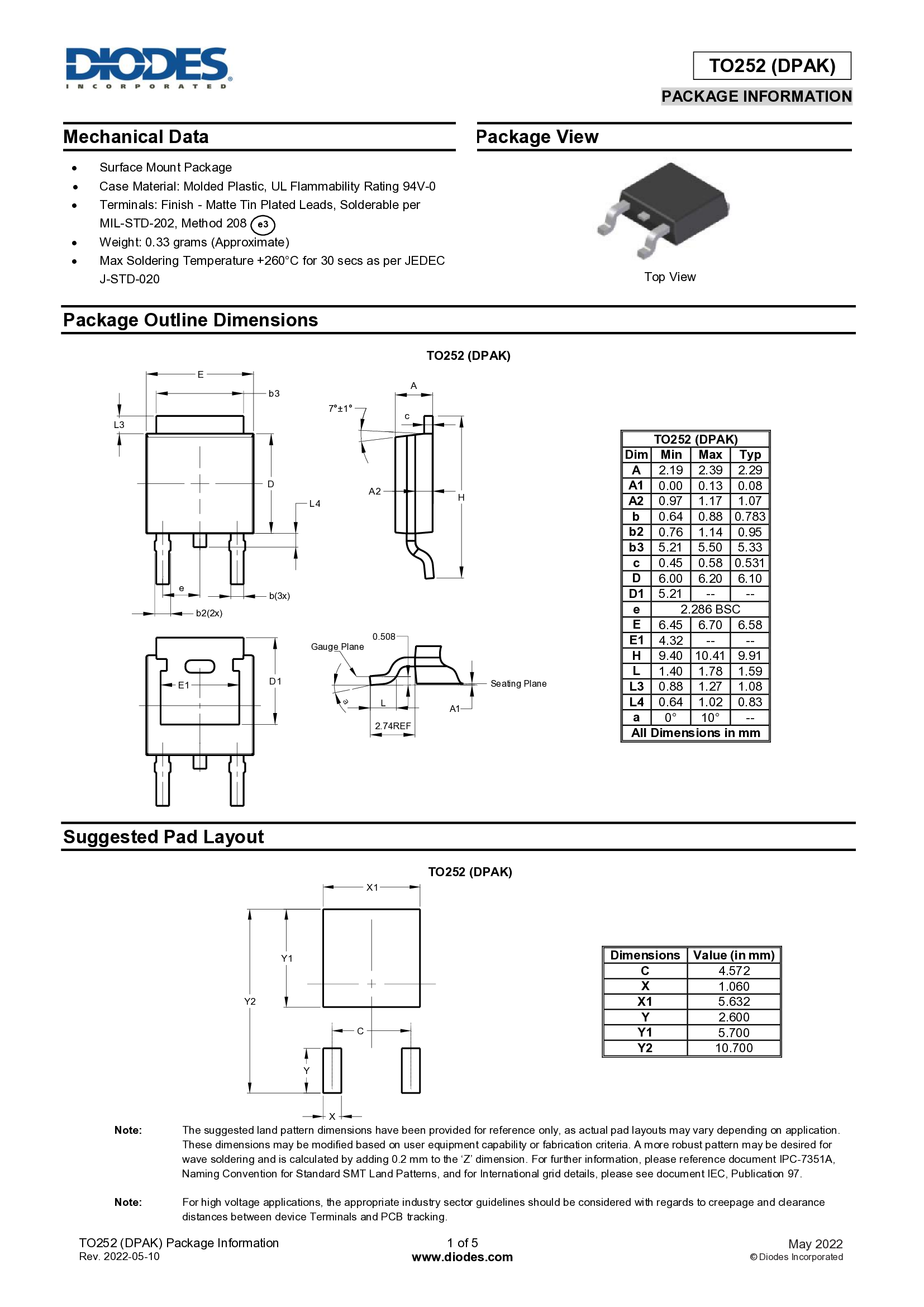
| Package | TO-252-2L (DPAK) | Surface-mount |
| Stock Availability | 15,466 units | Moderate availability |
| Unit Price | $0.11 | JLCPCB pricing |
| Output Voltage | -12V ±4% | -11.52V to -12.48V |
| Output Current | 1.5A max | Design uses 0.8A |
| Dropout Voltage | ~2V typical | Maximum VIN = -14V |
| Line Regulation | ±0.5% typical | Input voltage variation |
| Load Regulation | ±1% typical | Output current variation |
| Ripple Rejection | >60dB | @120Hz |
| Quiescent Current | ~5mA typical | No-load consumption |
| Thermal Resistance θJC | 5°C/W | Junction to case (tab) |
| Thermal Resistance θJA | 40°C/W | Junction to ambient |
| Operating Temp Range | 0°C to +125°C | Junction temperature |
Pin Configuration
         TO-252-2L (DPAK) Package
              Top View

         ┌──────────────┐
         │              │
         │    CJ7912    │
         │              │
         │              │
         │              │
         └──┬───────┬───┘
            │       │
          PIN1    PIN2
           GND    INPUT
        (Common) (-13.5V)

              TAB
           (OUTPUT)
            (-12V)

         Side View

         ┌──────────────┐
         │   Component  │ ← Surface mount IC
         └──┬───────┬───┘
            │       │
          PIN1    PIN2

    ════════════════════  ← Metal tab (OUTPUT)
                            soldered to PCB pad
Pin Descriptions
| Pin | Name | Function | Connection in Design |
|---|---|---|---|
| 1 | GND | Ground reference (common) | System ground plane |
| 2 | INPUT | Unregulated input voltage | -13.5V from DC-DC converter (U4) |
| TAB | OUTPUT | Regulated -12V output (metal tab) | -12V rail with protection circuit |
Critical Note: This is a NEGATIVE voltage regulator. Pin numbering and voltage polarities are different from positive regulators:
Pin 1 is GND (not INPUT like 78xx series)
Pin 2 is INPUT (not GND like 78xx series)
More negative voltage is "higher" voltage for this regulator
Input must be more negative than output (-13.5V is "higher" than -12V)
Application Circuit
-13.5V (from DC-DC) ──┬─── C13: 470nF ───┬─── U8: CJ7912 ────┬─── C16: 100nF ───┬─→ -12V OUT
                      │                  │                   │                  │
                      │                  │    ┌──────────┐   │                  │
                      │                  └────│2  INPUT  │   │                  │
                      │                       │          │   │                  │
                      │                    ┌──│1   GND   │   │                  │
                      │                    │  │          │   │                  │
                      │                    │  │   TAB ───┴───┴──────────────────┤
                      │                    │  └──────────┘                      │
                      │                    │     (OUTPUT)                       │
                      └─── C21: 470µF ─────┼─────────┬─── C22: 470µF ───────────┤
                           (Input)         │         │    (Output)              │
                                           │         │                          │
                                          GND       GND                         │
                                                                                │
                                        ┌───────────────────────────────────────┘
                                        │
                                  ┌─────┴─────┐
                                  │   LED4    │ Red Status LED
                                  │   (Red)   │ via R9: 1kΩ
                                  └─────┬─────┘
                                        │
                                       GND
Component Values
Input Capacitors
| Reference | Value | Type | Voltage | Package | Part Number | Purpose |
|---|---|---|---|---|---|---|
| C13 | 470nF | Ceramic X7R | 25V | 0603 | C1623 | High-frequency noise filtering |
| C21 | 470µF | Electrolytic | 25V | D10xL10.2mm | C3351 | Input voltage stabilization |
Important: For C21, negative terminal connects to -13.5V input, positive terminal connects to GND.
Output Capacitors
| Reference | Value | Type | Voltage | Package | Part Number | Purpose |
|---|---|---|---|---|---|---|
| C16 | 100nF | Ceramic X7R | 50V | 0805 | C1711 | High-frequency decoupling |
| C22 | 470µF | Electrolytic | 25V | D10xL10.2mm | C3351 | Load transient response |
Important: For C22, negative terminal connects to -12V output, positive terminal connects to GND.
Status LED Circuit
| Reference | Part | Value | Package | Part Number | Purpose |
|---|---|---|---|---|---|
| LED4 | Red LED | 2.0V @ 10mA | 0805 | C84256 | Power status indicator |
| R9 | Resistor | 1kΩ | 0603 | C21190 | LED current limiting |
LED Connection: Anode to GND, Cathode to -12V through R9 (reverse of positive rail LEDs).
Design Considerations
Negative Voltage Concepts
Understanding negative voltage regulators:
Voltage Levels (relative to GND = 0V):

                GND (0V) ─────────────────
                  │
                  │ +13.5V "above" ground
                  │
              +13.5V ─────────────────

                GND (0V) ─────────────────
                  │
                  │ 12V "below" ground
                  │
              -12V ─────────────────
                  │
                  │ 13.5V "below" ground
                  │
              -13.5V ─────────────────

For negative regulator:
- INPUT = -13.5V (more negative)
- OUTPUT = -12V (less negative)
- Dropout = |VIN| - |VOUT| = 13.5V - 12V = 1.5V
Input Voltage Requirements
The CJ7912 requires input voltage to be at least 2V more negative than the output for proper regulation:
Input voltage: -13.5V from LM2596S DC-DC converter
Output voltage: -12V
Dropout margin: 13.5V - 12V = 1.5V
Status: ⚠️ Marginal - operates near minimum dropout voltage
The 1.5V margin is slightly below the typical 2V dropout specification but acceptable because:
The DC-DC stage is regulated at -13.5V
The CJ7912 can regulate with 1.5V dropout at lower currents
Actual load current (0.8A) is well below maximum rating (1.5A)
Negative regulators often have slightly lower dropout than positive equivalents
Recommendation: For production, consider increasing DC-DC output to -14.0V for better dropout margin.
Thermal Management
Power dissipation calculation:
P = (|VIN| - |VOUT|) × IOUT
P = (13.5V - 12V) × 0.8A
P = 1.5V × 0.8A
P = 1.2W
Temperature rise without additional heatsinking:
ΔT =At 25°C ambient, junction temperature = 73°C (well within 125°C maximum).
Thermal performance of TO-252-2L:
Moderate θJA (40°C/W)
Metal tab provides good heat spreading
Direct thermal contact with PCB copper pour
No additional heatsink required for this application
PCB copper area recommendations:
Minimum: 3 cm² copper pour connected to tab
Recommended: 6 cm² copper pour for better margin
Thermal vias: 6-8 vias (0.3mm) under tab to bottom layer
Capacitor Placement and Polarity
Critical for negative regulators: Electrolytic capacitor polarity is REVERSED from what you might expect:
Correct polarity for negative rail:

C21 (Input, 470µF):
         ┌─────────┐
  GND ───┤+       -├─── -13.5V
         └─────────┘

C22 (Output, 470µF):
         ┌─────────┐
  GND ───┤+       -├─── -12V
         └─────────┘

REMEMBER:
- Positive terminal goes to GROUND (0V)
- Negative terminal goes to negative voltage
- This is OPPOSITE of positive voltage regulators
Placement guidelines:
C13 (470nF ceramic): Place within 5mm of pin 2
Purpose: Suppress high-frequency noise from DC-DC stage
Non-polarized, so no polarity concerns
C21 (470µF electrolytic): Place within 10mm of pin 2
Purpose: Stabilize input voltage during load transients
POLARITY: + to GND, - to -13.5V
C16 (100nF ceramic): Place within 5mm of output tab
Purpose: High-frequency output decoupling
Critical for preventing oscillation
C22 (470µF electrolytic): Place within 10mm of output tab
Purpose: Improve load transient response
POLARITY: + to GND, - to -12V
Ground Plane Connection
The TO-252-2L package layout:
Pin 1 (GND): Wide connection directly to ground plane
Pin 2 (INPUT): Connect to -13.5V rail
Tab (OUTPUT): Large copper pour for -12V distribution and thermal management
Thermal vias: Essential for heat dissipation to inner/bottom layers
Performance Characteristics
Regulation Performance
| Condition | Specification | Typical Performance |
|---|---|---|
| Line regulation | VIN = -14.5V to -27V | ±0.5% (±60mV) |
| Load regulation | IOUT = 5mA to 1.5A | ±1% (±120mV) |
| Output voltage accuracy | At 25°C | ±4% (±480mV) |
| Temperature coefficient | -40°C to +125°C | ±1mV/°C typical |
Noise Performance
| Parameter | Value | Conditions |
|---|---|---|
| Ripple rejection | 60dB min | f = 120Hz |
| Output noise voltage | <1mVp-p | With recommended capacitors |
| Transient response | <50µs | 400mA load step |
Protection Features
Built-in Protections
Thermal Shutdown: Automatically shuts down if junction temperature exceeds 150°C
Short Circuit Protection: Current limiting prevents damage during output short
Safe Operating Area (SOA): Internal circuitry ensures operation within safe limits
External Protection (This Design)
-12V (from U8) ──┬─── PTC3: 1.1A ──┬─── F3: 1.5A ──┬─── TVS3: SMAJ15A ───┬─→ -12V OUT
                 │  (Auto-Reset)   │   (Backup)    │  (15V Clamp Rev)    │
                 │                 │               │      ↑              │
                 │                 │               └─────GND─────────────┤
                 │                 │                                     │
                 └─── LED4 (Red) via R9 (1kΩ) ──────────────→ Power Status
                      (Cathode to -12V, Anode to GND through resistor)
TVS Diode Connection for Negative Rail:
         TVS3 (SMAJ15A)
            ┌─────┐
-12V ───────┤  │  ├────── GND
            └──▲──┘
               │
          (Cathode to -12V
           Anode to GND)
Protection stages:
Overload (0.9A-1.5A): PTC3 trips → Auto-reset after cooling
Short circuit (>1.5A): F3 blows → Manual replacement required
Overvoltage: TVS3 clamps transients (reverse-biased for negative voltage)
Note: For the negative rail, the TVS diode is connected with cathode to -12V and anode to GND, which is reverse of positive rail configuration.
Bill of Materials
| Designator | Part | Value | Package | JLCPCB Part # | Qty | Unit Price | Extended |
|---|---|---|---|---|---|---|---|
| U8 | CJ7912 | Fixed -12V LDO | TO-252-2L | C94173 | 1 | $0.11 | $0.11 |
| C13 | Ceramic Cap | 470nF 25V X7R | 0603 | C1623 | 1 | $0.0036 | $0.0036 |
| C16 | Ceramic Cap | 100nF 50V X7R | 0805 | C1711 | 1 | $0.0021 | $0.0021 |
| C21, C22 | Electrolytic | 470µF 25V | D10xL10.2mm | C3351 | 2 | $0.044 | $0.088 |
| LED4 | LED | Red 0805 | 0805 | C84256 | 1 | $0.0126 | $0.0126 |
| R9 | Resistor | 1kΩ ±1% | 0603 | C21190 | 1 | $0.0005 | $0.0005 |
| Total | $0.22 |
Note: Higher total cost than positive regulators due to larger electrolytic capacitors (25V rating vs 10V).
Alternative Parts
Direct Replacements (TO-252-2L Package)
| Part Number | Manufacturer | JLCPCB Part # | Stock | Price | Notes |
|---|---|---|---|---|---|
| CJ7912 | Jiangsu Changjing Electronics | C94173 | 15,466 | $0.11 | Recommended (moderate stock) |
| LM7912DT | STMicroelectronics | Check | Check | ~$0.15 | Higher quality, better specs |
| MC7912DTG | ON Semiconductor | Check | Check | ~$0.14 | Pin-compatible |
Package Alternatives
| Package | Part Number | JLCPCB Part # | Stock | Price | Notes |
|---|---|---|---|---|---|
| TO-252-2L | CJ7912 | C94173 | 15,466 | $0.11 | Recommended (SMD) |
| TO-220 | L7912CV | C192101 | 3,386 | $0.11 | Through-hole alternative |
| SOT-89 | LM7912-SOT89 | Check | Lower | ~$0.18 | Lower current rating |
Stock Note: If C94173 (CJ7912) is out of stock, consider C192101 (L7912CV TO-220) which has similar availability.
PCB Layout Guidelines
Footprint Requirements
TO-252-2L (DPAK) package footprint specifications:
         Top View (PCB Pad Layout)

    ┌──────────────────────────────┐
    │                              │
    │    Large Copper Pour         │  ← OUTPUT TAB (-12V)
    │    (6cm² recommended)        │     thermal + electrical
    │                              │
    │         Thermal Vias         │
    │         (6-8 vias)           │
    │                              │
    └──────────────────────────────┘

         PIN1 ■        PIN2 ■
         (GND)       (INPUT)
                    (-13.5V)

    Pin spacing: 2.28mm
    Pin pad: 1.5mm x 2.0mm
    Tab pad: 10mm x 10mm (minimum)
            12mm x 12mm (recommended)
Recommended Pad Dimensions
| Pad | Width | Length | Purpose |
|---|---|---|---|
| Pin 1 (GND) | 2.0mm | 3.0mm | Larger for ground connection |
| Pin 2 (INPUT) | 1.5mm | 2.0mm | Solder pad for input pin |
| Tab (OUTPUT) | 10-12mm | 10-12mm | Thermal and electrical connection |
Layout Recommendations
Component placement:
Orient IC with tab facing interior of PCB
Maximize copper area under and around tab for -12V rail
Keep input and output capacitors on same side as regulator
Separate -12V copper pour from +12V pour (clearance >2mm)
Copper pours:
Create dedicated copper pour for -12V rail (6cm² minimum)
Top layer: Main output pad and distribution to -12V loads
Bottom layer: Additional copper connected via thermal vias
Keep -12V copper separate from positive voltage pours
Thermal vias:
Place 6-8 thermal vias (0.3mm diameter) under tab
Arrange in grid pattern for even heat distribution
Connect to bottom layer copper pour for -12V
Direct connection (no thermal relief) for best heat transfer
Trace widths:
Input trace (-13.5V): 0.8mm minimum (0.8A current)
Output trace (-12V): 1mm minimum (0.8A current)
Ground: Maximum copper pour area
High-current paths: 2mm or copper pour preferred
Electrolytic capacitor polarity markings:
Add clear silkscreen markings: "+" toward GND
Add polarity indicators to prevent assembly errors
Consider adding text: "NEG RAIL - CHECK POLARITY"
Critical Layout Warnings
⚠️  ELECTROLYTIC CAPACITOR POLARITY WARNING ⚠️

For negative voltage regulator:
  Positive terminal (+) → GND (0V)
  Negative terminal (-) → Negative voltage

This is OPPOSITE of positive regulators!

Add clear silkscreen markings to prevent
assembly errors that will destroy capacitors.
Thermal Via Pattern
    Recommended thermal via pattern
    under TO-252-2L tab:

    ┌─────────────────────────┐
    │                         │
    │  ●    ●    ●    ●    ●  │
    │                         │  ← 0.3mm vias
    │  ●    ●    ●    ●    ●  │     2.5mm spacing
    │                         │
    └─────────────────────────┘

    Total vias: 10 (aggressive cooling)
    Minimum: 6 vias
    Recommended: 8 vias
Assembly Considerations
Critical Assembly Warnings
ELECTROLYTIC CAPACITOR POLARITY:
The most common assembly error with negative voltage regulators is installing electrolytic capacitors backwards. This will cause:
Immediate capacitor failure
Possible explosion of electrolytic capacitors
Regulator damage
Board contamination
Prevention:
Add clear silkscreen markings on PCB
Include assembly notes in BOM
Test capacitor polarity with DMM before powering
Use polarized ceramic capacitors if available (more expensive)
Soldering Guidelines
Reflow soldering (recommended for production):
Peak temperature: 260°C maximum
Time above 220°C: 60-90 seconds
Solder paste: SAC305 or similar lead-free
Stencil thickness: 0.125mm (5 mil)
Hand soldering:
Soldering iron: 350°C maximum
Solder pin 1 (GND) first for reference
Solder pin 2 (INPUT) second
Apply solder to tab from component side
Ensure good thermal contact between tab and PCB pad
Inspection Points
After assembly, inspect:
Electrolytic capacitor polarity: CRITICAL - verify + to GND
Pin solder joints: Smooth fillet, no bridges
Tab solder joint: Good coverage, no voids
Component alignment: Centered on pads
Thermal via filling: Solder should wick into vias
Pre-power checklist:
[ ] C21 polarity: + terminal to GND, - terminal to -13.5V
[ ] C22 polarity: + terminal to GND, - terminal to -12V
[ ] Visual inspection complete
[ ] Continuity test: GND to pin 1
[ ] Resistance test: No shorts between -12V and GND
[ ] Resistance test: No shorts between -13.5V and GND
Testing and Validation
Pre-Power Inspection
Before applying power, verify:
Capacitor polarity check:
C21: Measure with DMM in diode mode
C22: Measure with DMM in diode mode
Positive terminal should be at GND potential
Negative terminal should be connected to negative voltage rail
Visual inspection:
No solder bridges
Good solder joints on tab
Correct IC orientation
All components present
Initial Power-Up Test
Apply input voltage slowly:
Start with -10V input (below regulation threshold)
Gradually increase to -13.5V
Monitor for smoke or unusual smells
Check for thermal runaway
No-load test:
Apply -13.5V to input
Verify output voltage: -11.52V to -12.48V (-12V ±4%)
Measure quiescent current: <10mA
Check case temperature: Should be near ambient
Load Regulation Test
Connect variable load (0-1.0A)
Measure output voltage at different load currents:
0mA: Should be within -12V ±2%
400mA: Should be within -12V ±3%
800mA: Should be within -12V ±4%
Verify voltage variation <120mV from no-load to full-load
Thermal Test
Apply 0.8A load for 30 minutes
Measure case temperature with thermal camera
Verify case temperature <75°C at 25°C ambient
Compare to calculation: Should be ~73°C
Check for thermal shutdown (should not occur)
Ripple and Noise Test
Connect oscilloscope (AC coupling, 20MHz bandwidth limit)
Use short ground lead or coax probe
Measure output relative to GND with 0.8A load
Verify peak-to-peak ripple <5mVp-p (target: <1mVp-p)
Check for oscillation or instability
Transient Response Test
Use electronic load with step function (0A → 0.8A)
Monitor output voltage on oscilloscope
Verify voltage dip <200mV during load step
Verify recovery time <100µs
Check for ringing or overshoot
Troubleshooting
| Symptom | Possible Cause | Solution |
|---|---|---|
| No output voltage | Input voltage not negative enough | Verify -13.5V input from DC-DC |
| Shorted output | Check for shorts on -12V rail | |
| Electrolytic cap installed backwards | CHECK POLARITY - replace if backwards | |
| Thermal shutdown | Reduce load, check thermal vias | |
| Smoke/burning smell | Electrolytic cap reversed | POWER OFF IMMEDIATELY - replace cap |
| Output shorted to ground | Remove short, check board | |
| Low output magnitude | Insufficient input voltage | Check DC-DC output (should be -13.5V) |
| (e.g., -10V instead of -12V) | Excessive load current | Verify load <0.8A |
| Poor ground connection | Check pin 1 connection | |
| High ripple noise | Missing input capacitor | Verify C13, C21 installed |
| Missing output capacitor | Verify C16, C22 installed | |
| Wrong capacitor polarity | Check electrolytic polarity | |
| Oscillation | Missing C16 (100nF output) | Add C16 close to output tab |
| Long output traces | Shorten traces, add local decoupling | |
| Capacitive load | Add series resistance (1Ω) at output | |
| Overheating | Excessive power dissipation | Check input voltage (should be -13.5V) |
| Insufficient copper area | Increase copper pour under tab | |
| No thermal vias | Add thermal vias under tab | |
| Poor thermal contact | Check solder joint on tab | |
| Wrong polarity output | Wrong regulator installed | Verify CJ7912 not CJ7812 |
| (+12V instead of -12V) | Wiring error | Check schematic vs. layout |
| Voltage too negative | Input voltage too negative | Check DC-DC stage (-13.5V target) |
| (e.g., -13V instead of -12V) | Wrong feedback resistors on DC-DC | Check U4 feedback network |
Application Notes
Op-Amp Power Supply Considerations
The -12V rail typically powers operational amplifiers in modular synthesizers:
Typical op-amp requirements:
Dual supply: ±12V (some designs use ±15V)
Current per op-amp: 2-10mA quiescent
Peak current: Up to 30mA during output swings
Noise sensitivity: Very high (audio applications)
Distribution recommendations:
Star ground topology:
Connect all op-amp ground pins to single point
Prevents ground loops and noise coupling
Keep analog ground separate from digital ground
Local decoupling:
Add 100nF ceramic capacitor at each op-amp power pin
Place capacitor within 5mm of IC
Both +12V and -12V pins need decoupling
Bulk capacitance:
Add 10µF electrolytic per 4-8 op-amps
Place in central location
Remember polarity: + to GND, - to -12V
Audio Noise Considerations
For ultra-low-noise audio applications:
Additional filtering:
Add RC filter: 10Ω + 47µF per audio section
Creates pole at ~340Hz
Reduces regulator noise in audio band
Separate analog/digital -12V:
Use separate regulators if possible
If sharing regulator, use isolation filters
Prevents digital switching noise coupling to audio circuits
PCB layout:
Keep -12V traces away from high-frequency signals
Use ground plane as shield
Route audio signals perpendicular to power traces
Dual Supply Voltage Matching
When using ±12V supplies for op-amps, voltage matching is important:
| Parameter | Specification | Impact |
|---|---|---|
| Voltage match | Within ±0.5V | Prevents DC offset in op-amp outputs |
| Noise match | Within 2:1 ratio | Balanced noise rejection |
| Regulation match | Within ±1% | Consistent performance across temperature |
Verification:
Measure both +12V and -12V outputs simultaneously
Calculate: |V+12| - |V-12| should be <0.5V
Adjust DC-DC stage if needed (modify feedback resistors)
Related Components
Upstream: LM2596S-ADJ (U4) - Provides -13.5V input via inverting buck-boost topology
Downstream: Protection circuit (PTC3, F3, TVS3)
Parallel regulators: L7812CD2T-TR (U6), L7805ABD2T-TR (U7)
Common Mistakes and How to Avoid Them
Mistake 1: Reversed Electrolytic Capacitors
Problem: Installing C21 or C22 with reversed polarity Consequence: Capacitor explosion, regulator damage Prevention:
Add large silkscreen warnings on PCB
Test polarity with DMM before powering up
Use checklist during assembly
Mistake 2: Confusing Positive and Negative Regulator Pinouts
Problem: Assuming pin 1 is INPUT (like 78xx series) Consequence: Wrong connections, no output Prevention:
Clearly label pins on schematic: "Pin 1 = GND" not "Pin 1"
Add reference designator table to schematic
Use different symbol for negative regulators
Mistake 3: Insufficient Dropout Voltage
Problem: Input voltage not negative enough (-12V input for -12V output) Consequence: No regulation, output follows input Prevention:
Calculate dropout: |VIN| must be >|VOUT| + 2V
Design DC-DC stage for -13.5V or -14V
Monitor DC-DC output voltage during testing
Mistake 4: Wrong TVS Diode Polarity
Problem: Installing TVS3 with cathode to GND (like positive rail) Consequence: No overvoltage protection, possible short circuit Prevention:
Clearly mark TVS polarity on schematic
For negative rail: Cathode to negative voltage, Anode to GND
Test TVS connection with DMM (should show high resistance GND to -12V)
Mistake 5: Shared Copper Pour with Positive Rails
Problem: Connecting -12V copper to +12V copper Consequence: Direct short circuit, catastrophic failure Prevention:
Use separate copper pours for each voltage rail
Maintain >2mm clearance between different voltage pours
Use DRC (Design Rule Check) to verify clearances
References
CJ7912 Datasheet - Jiangsu Changjing Electronics
Negative Voltage Regulator Application Note - Texas Instruments
LM79xx Series Datasheet - General reference for 79xx series
Related documentation: Diagram7 - -12V Linear Regulator