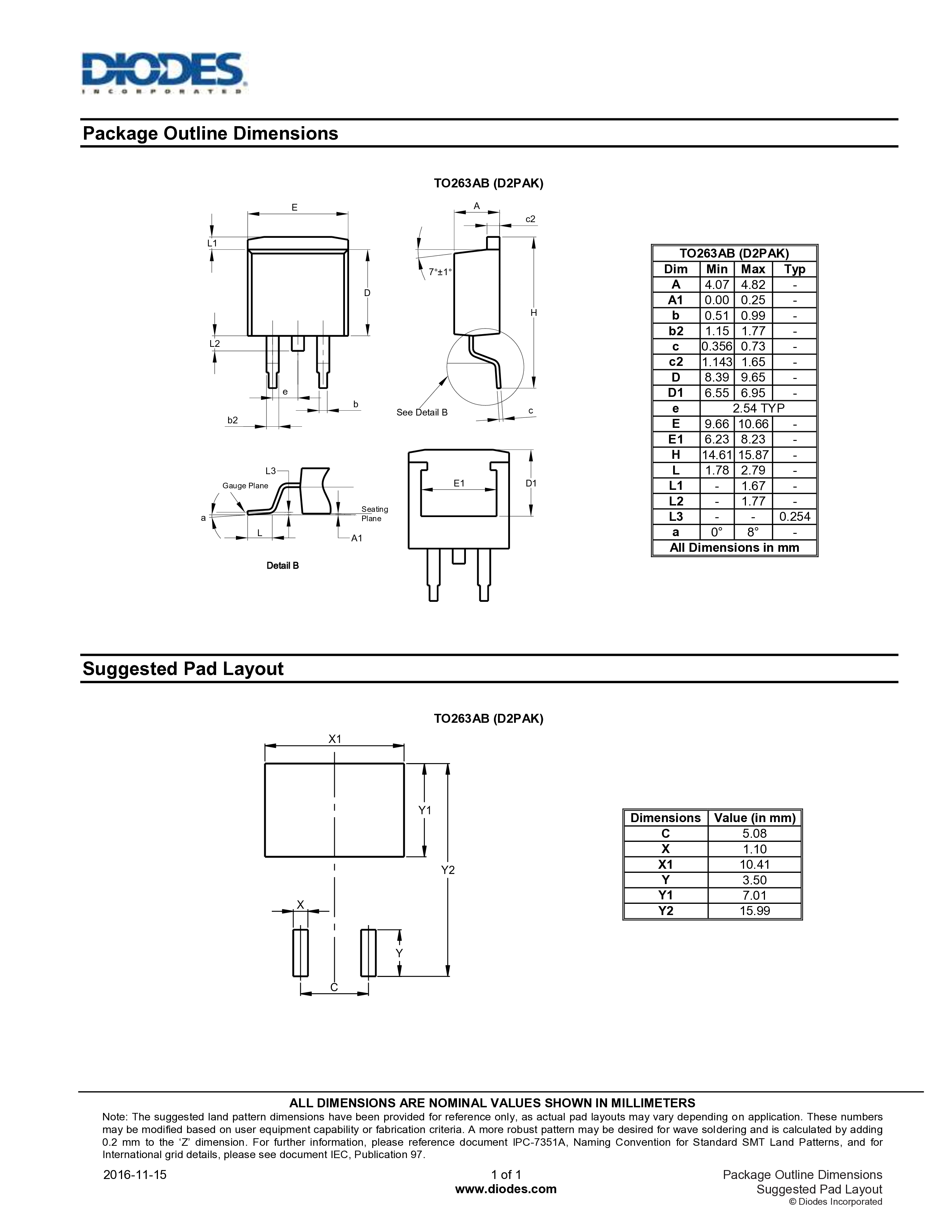
L7805ABD2T-TR - +5V Linear Regulator
Fixed positive voltage regulator providing stable +5V output in compact TO-263-2 (D2PAK) surface-mount package with excellent thermal performance.

Overview
The L7805ABD2T-TR is a three-terminal positive voltage regulator in TO-263-2 (D2PAK) package, designed to provide a fixed +5V output from a higher input voltage. This component serves as the final stage in the +5V power rail, converting the +7.5V DC-DC output to a clean, low-noise +5V suitable for modular synthesizer digital circuits and control voltage applications.
Key Specifications
| Parameter | Value | Notes |
|---|---|---|
| JLCPCB Part Number | C86206 | |
| Manufacturer Part Number | L7805ABD2T-TR | |
| Package | TO-263-2 (D2PAK) | Surface-mount |
| Stock Availability | 272,379 units | Very high availability |
| Unit Price | $0.11 | JLCPCB pricing |
| Output Voltage | 5V ±4% | 4.8V - 5.2V |
| Output Current | 1.5A max | Design uses 0.5A |
| Dropout Voltage | ~2V typical | Minimum VIN = 7V |
| Line Regulation | ±0.5% typical | Input voltage variation |
| Load Regulation | ±1% typical | Output current variation |
| Ripple Rejection | >60dB | @120Hz |
| Quiescent Current | ~5mA typical | No-load consumption |
| Thermal Resistance θJC | 3°C/W | Junction to case (tab) |
| Thermal Resistance θJA | 35°C/W | Junction to ambient |
| Operating Temp Range | 0°C to +125°C | Junction temperature |
Pin Configuration
         TO-263-2 (D2PAK) Package
              Top View

         ┌──────────────┐
         │              │
         │   L7805A     │
         │   BD2T-TR    │
         │              │
         │              │
         └──┬───────┬───┘
            │       │
          PIN1    PIN2
          INPUT    GND
         (+7.5V) (Common)

              TAB
           (OUTPUT)
            (+5V)

         Side View

         ┌──────────────┐
         │   Component  │ ← Surface mount IC
         └──┬───────┬───┘
            │       │
          PIN1    PIN2

    ════════════════════  ← Metal tab (OUTPUT)
                            soldered to PCB pad
Pin Descriptions
| Pin | Name | Function | Connection in Design |
|---|---|---|---|
| 1 | INPUT | Unregulated input voltage | +7.5V from DC-DC converter (U3) |
| 2 | GND | Ground reference (common) | System ground plane |
| TAB | OUTPUT | Regulated +5V output (metal tab) | +5V rail with protection circuit |
Note: Unlike TO-220 package, the TO-263-2 has the OUTPUT on the metal tab, not on pin 3.
Application Circuit
+7.5V (from DC-DC) ───┬─── C12: 470nF ───┬─── U7: L7805ABD2T ───┬─── C15: 100nF ───┬─→ +5V OUT
                      │                  │                      │                  │
                      │                  │    ┌──────────┐      │                  │
                      │                  └────│1  INPUT  │      │                  │
                      │                       │          │      │                  │
                      │                    ┌──│2   GND   │      │                  │
                      │                    │  │          │      │                  │
                      │                    │  │   TAB ───┴──────┴──────────────────┤
                      │                    │  └──────────┘                         │
                      │                    │     (OUTPUT)                          │
                      └─── C19: 470µF ─────┼─────────┬─── C20: 470µF ──────────────┤
                           (Input)         │         │    (Output)                 │
                                           │         │                             │
                                          GND       GND                            │
                                                                                   │
                                        ┌──────────────────────────────────────────┘
                                        │
                                  ┌─────┴─────┐
                                  │   LED3    │ Blue Status LED
                                  │  (Blue)   │ via R8: 1kΩ
                                  └─────┬─────┘
                                        │
                                       GND
Component Values
Input Capacitors
| Reference | Value | Type | Voltage | Package | Part Number | Purpose |
|---|---|---|---|---|---|---|
| C12 | 470nF | Ceramic X7R | 25V | 0603 | C1623 | High-frequency noise filtering |
| C19 | 470µF | Electrolytic | 10V | D6.3xL7.7mm | C335982 | Input voltage stabilization |
Output Capacitors
| Reference | Value | Type | Voltage | Package | Part Number | Purpose |
|---|---|---|---|---|---|---|
| C15 | 100nF | Ceramic X7R | 50V | 0805 | C1711 | High-frequency decoupling |
| C20 | 470µF | Electrolytic | 10V | D6.3xL7.7mm | C335982 | Load transient response |
Status LED Circuit
| Reference | Part | Value | Package | Part Number | Purpose |
|---|---|---|---|---|---|
| LED3 | Blue LED | 2.8V @ 10mA | 0805 | C72041 | Power status indicator |
| R8 | Resistor | 1kΩ | 0603 | C21190 | LED current limiting |
Design Considerations
Input Voltage Requirements
The L7805ABD2T requires a minimum input voltage of approximately 7V for proper regulation (5V output + 2V dropout). In this design:
Input voltage: +7.5V from LM2596S DC-DC converter
Dropout margin: 7.5V - 5V = 2.5V
Status: ✅ Excellent - well above minimum dropout voltage
The 2.5V margin provides:
Stable regulation across load variations
Tolerance for input voltage ripple
Reduced power dissipation compared to higher input voltages
Optimal efficiency for the linear regulator stage
Thermal Management
Power dissipation calculation:
P = (VIN - VOUT) × IOUT
P = (7.5V - 5V) × 0.5A
P = 2.5V × 0.5A
P = 1.25W
Temperature rise without additional heatsinking:
ΔT =At 25°C ambient, junction temperature = 68.75°C (well within 125°C maximum).
Thermal performance advantages of TO-263-2:
Lower θJA than TO-220 (35°C/W vs 50°C/W)
Large metal tab provides excellent heat spreading
Direct thermal contact with PCB copper pour
No additional heatsink required for this application
PCB copper area recommendations:
Minimum: 2 cm² copper pour connected to tab
Recommended: 5 cm² copper pour for better margin
Thermal vias: 6-10 vias (0.3mm) under tab to bottom layer
Capacitor Placement
Critical for stability and noise rejection:
C12 (470nF ceramic): Place within 5mm of pin 1
Purpose: Suppress high-frequency noise from DC-DC stage
Type: X7R or better (maintains capacitance vs. temperature)
C19 (470µF electrolytic): Place within 10mm of pin 1
Purpose: Stabilize input voltage during load transients
Polarity: Positive terminal to input, negative to ground
C15 (100nF ceramic): Place within 5mm of output tab
Purpose: High-frequency output decoupling
Critical for preventing oscillation
Must be ceramic for low ESR/ESL
C20 (470µF electrolytic): Place within 10mm of output tab
Purpose: Improve load transient response
ESR: <2Ω for best performance
Helps with sudden current demands
Ground Plane Connection
The TO-263-2 package requires careful PCB layout:
Pin 2 (GND): Connect directly to ground plane with wide trace
Tab (OUTPUT): Large copper pour for both electrical and thermal connection
Thermal vias: Essential for heat dissipation to inner/bottom layers
Keep-out area: Maintain clearance around pins for solder inspection
Performance Characteristics
Regulation Performance
| Condition | Specification | Typical Performance |
|---|---|---|
| Line regulation | VIN = 7V to 25V | ±0.5% (±25mV) |
| Load regulation | IOUT = 5mA to 1.5A | ±1% (±50mV) |
| Output voltage accuracy | At 25°C | ±4% (±200mV) |
| Temperature coefficient | -40°C to +125°C | ±1mV/°C typical |
Noise Performance
| Parameter | Value | Conditions |
|---|---|---|
| Ripple rejection | 60dB min | f = 120Hz |
| Output noise voltage | <1mVp-p | With recommended capacitors |
| Transient response | <50µs | 250mA load step |
| PSRR (Power Supply Rejection) | >60dB | 100Hz - 10kHz |
Protection Features
Built-in Protections
Thermal Shutdown: Automatically shuts down if junction temperature exceeds 150°C
Short Circuit Protection: Current limiting prevents damage during output short
Safe Operating Area (SOA): Internal circuitry ensures operation within safe limits
Reverse Polarity: Input diode protects against reverse voltage
External Protection (This Design)
+5V (from U7) ───┬─── PTC2: 1.1A ───┬─── F2: 1.5A ──┬─── TVS2: SD05 ────────┬─→ +5V OUT
                 │  (Auto-Reset)    │   (Backup)    │   (5V Clamp)          │
                 │                  │               │      ↕                │
                 │                  │               └─────GND────────────────┤
                 │                  │                                       │
                 └─── LED3 (Blue) via R8 (1kΩ) ──────────────→ Power Status
Protection stages:
Overload (0.6A-1.5A): PTC2 trips → Auto-reset after cooling
Short circuit (>1.5A): F2 blows → Manual replacement required
Overvoltage: TVS2 clamps transients above 6V (unidirectional)
Note: The TVS2 (SD05) is unidirectional, optimized for positive DC power rail protection.
Bill of Materials
| Designator | Part | Value | Package | JLCPCB Part # | Qty | Unit Price | Extended |
|---|---|---|---|---|---|---|---|
| U7 | L7805ABD2T-TR | Fixed +5V LDO | TO-263-2 | C86206 | 1 | $0.11 | $0.11 |
| C12 | Ceramic Cap | 470nF 25V X7R | 0603 | C1623 | 1 | $0.0036 | $0.0036 |
| C15 | Ceramic Cap | 100nF 50V X7R | 0805 | C1711 | 1 | $0.0021 | $0.0021 |
| C19, C20 | Electrolytic | 470µF 10V | D6.3xL7.7mm | C335982 | 2 | $0.014 | $0.028 |
| LED3 | LED | Blue 0805 | 0805 | C72041 | 1 | $0.0126 | $0.0126 |
| R8 | Resistor | 1kΩ ±1% | 0603 | C21190 | 1 | $0.0005 | $0.0005 |
| Total | $0.16 |
Alternative Parts
Direct Replacements (TO-263-2 Package)
| Part Number | Manufacturer | JLCPCB Part # | Stock | Price | Notes |
|---|---|---|---|---|---|
| L7805ABD2T-TR | STMicroelectronics | C86206 | 272,379 | $0.11 | Recommended (very high stock) |
| MC7805BD2T | ON Semiconductor | Check | Check | ~$0.12 | Pin-compatible |
| UA7805CKC | Texas Instruments | Check | Check | ~$0.13 | Pin-compatible |
Package Alternatives
| Package | Part Number | JLCPCB Part # | Stock | Price | Notes |
|---|---|---|---|---|---|
| TO-263-2 | L7805ABD2T-TR | C86206 | 272,379 | $0.11 | Recommended (best thermal) |
| TO-220 | L7805CV | C2846 | 55,629 | $0.11 | Through-hole alternative |
| SOT-89 | AMS1117-5.0 | C6187 | High | $0.05 | Lower current (1A max) |
Recommendation: Stick with TO-263-2 for SMD assembly and superior thermal performance.
PCB Layout Guidelines
Footprint Requirements
TO-263-2 (D2PAK) package footprint specifications:
         Top View (PCB Pad Layout)

    ┌──────────────────────────────┐
    │                              │
    │    Large Copper Pour         │  ← OUTPUT TAB
    │    (5cm² recommended)        │     thermal + electrical
    │                              │
    │         Thermal Vias         │
    │         (6-10 vias)          │
    │                              │
    └──────────────────────────────┘

         PIN1 ■        PIN2 ■
        (INPUT)        (GND)

    Pin spacing: 2.54mm (0.1")
    Pin pad: 1.5mm x 2.0mm
    Tab pad: 10mm x 10mm (minimum)
            15mm x 15mm (recommended)
Recommended Pad Dimensions
| Pad | Width | Length | Purpose |
|---|---|---|---|
| Pin 1 (INPUT) | 1.5mm | 2.0mm | Solder pad for input pin |
| Pin 2 (GND) | 2.0mm | 3.0mm | Larger for ground connection |
| Tab (OUTPUT) | 10-15mm | 10-15mm | Thermal and electrical connection |
Layout Recommendations
Component placement:
Orient IC with tab facing interior of PCB (away from edge)
Maximize copper area under and around tab
Keep input and output capacitors on same side as regulator
Copper pours:
Create large copper pour (5cm² minimum) connected to output tab
Top layer: Main output pad and distribution
Bottom layer: Additional copper connected via thermal vias
Inner layers (4-layer board): Additional ground/power planes
Thermal vias:
Place 6-10 thermal vias (0.3mm diameter) under tab
Arrange in grid pattern for even heat distribution
Connect to bottom layer copper pour
Do NOT use thermal relief on these vias (direct connection needed)
Via spacing: ~2mm apart
Trace widths:
Input trace (7.5V): 0.5mm minimum (0.5A current, low voltage drop)
Output trace (5V): 1mm minimum (0.5A current)
Ground: Maximum copper pour area
High-current paths: 2mm or copper pour preferred
Capacitor placement:
C12 ──┐  ┌── IC ──┐  ┌── C15
      │  │        │  │
C19 ──┘  │  U7    │  └── C20
         │        │
         └────────┘

Distance:
- C12: <5mm from pin 1
- C19: <10mm from pin 1
- C15: <5mm from output tab
- C20: <10mm from output tab
Thermal Via Pattern
    Recommended thermal via pattern
    under TO-263-2 tab:

    ┌─────────────────────────┐
    │  ●    ●    ●    ●    ●  │
    │                         │
    │  ●    ●    ●    ●    ●  │  ← 0.3mm vias
    │                         │     2mm spacing
    │  ●    ●    ●    ●    ●  │
    │                         │
    └─────────────────────────┘

    Total vias: 15 (aggressive cooling)
    Minimum: 6 vias
    Recommended: 10 vias
Assembly Considerations
Soldering Guidelines
Reflow soldering (recommended for production):
Peak temperature: 260°C maximum
Time above 220°C: 60-90 seconds
Solder paste: SAC305 or similar lead-free
Stencil thickness: 0.125mm (5 mil)
Hand soldering:
Soldering iron: 350°C maximum
Solder pin 1 and pin 2 first
Apply solder to tab from component side
Ensure good thermal contact between tab and PCB pad
Use generous solder for tab connection
Inspection Points
After assembly, inspect:
Pin solder joints: Smooth fillet, no bridges
Tab solder joint: Good coverage, no voids visible
Component alignment: Centered on pads
No cold solder joints: Shiny, smooth finish
Thermal via filling: Solder should wick into vias
Testing and Validation
Input Voltage Test
Apply 7.5V to input with no load
Verify output voltage: 4.8V - 5.2V (5V ±4%)
Measure quiescent current: <10mA
Load Regulation Test
Connect variable load (0-1.0A)
Measure output voltage at different load currents:
0mA: Should be within 5V ±2%
250mA: Should be within 5V ±3%
500mA: Should be within 5V ±4%
Verify voltage drop <50mV from no-load to full-load
Thermal Test
Apply 0.5A load for 30 minutes
Measure case temperature with thermal camera or thermocouple
Verify case temperature <70°C at 25°C ambient
Compare to calculation: Should be ~69°C
Check for thermal shutdown (should not occur)
Ripple and Noise Test
Connect oscilloscope (AC coupling, 20MHz bandwidth limit)
Use short ground lead or coax probe
Measure output with 0.5A load
Verify peak-to-peak ripple <5mVp-p (target: <1mVp-p)
Check for oscillation or instability (should be stable)
Transient Response Test
Use electronic load with step function (0A → 0.5A)
Monitor output voltage on oscilloscope
Verify voltage dip <250mV during load step
Verify recovery time <100µs
Check for ringing or overshoot
Troubleshooting
| Symptom | Possible Cause | Solution |
|---|---|---|
| No output voltage | Input voltage too low | Verify 7.5V input from DC-DC |
| Shorted output | Check for shorts on +5V rail | |
| Thermal shutdown | Reduce load, check thermal vias | |
| Poor tab solder joint | Reflow tab solder connection | |
| Low output voltage | Insufficient input voltage | Check DC-DC stage output (should be 7.5V) |
| Excessive load current | Verify load <0.5A (design spec) | |
| Poor ground connection | Check pin 2 and ground plane | |
| High trace resistance | Check trace widths and connections | |
| High ripple noise | Missing input capacitor | Verify C12, C19 installed correctly |
| Missing output capacitor | Verify C15, C20 installed correctly | |
| Poor capacitor placement | Move capacitors closer to IC | |
| Ground loop issues | Check ground plane continuity | |
| Oscillation | Missing C15 (100nF output) | Add C15 close to output tab |
| Long output traces | Shorten traces, add local decoupling | |
| Capacitive load | Add series resistance (1Ω) at output | |
| Poor ground routing | Improve ground plane connections | |
| Overheating | Excessive power dissipation | Check input voltage (should be 7.5V) |
| Insufficient copper area | Increase copper pour under tab | |
| No thermal vias | Add thermal vias under tab | |
| Poor thermal contact | Check solder joint on tab | |
| Voltage too high | Wrong regulator installed | Verify L7805A not L7812 or other |
| Open feedback loop | Check internal IC (unlikely) | |
| Voltage too low | Input voltage marginal | Verify 7.5V input stable |
| Excessive load | Reduce load current |
Application Notes
Digital vs. Analog Loads
The +5V rail in modular synthesizers may power:
Digital circuits (microcontrollers, logic ICs):
Characteristics: Switching loads, transient currents
Decoupling: Add 100nF ceramic capacitor at each IC
Distribution: Star topology from main filter cap
Analog circuits (op-amps, comparators):
Characteristics: Steady loads, noise-sensitive
Decoupling: 100nF ceramic + 10µF electrolytic per section
Isolation: Consider RC filter if needed (10Ω + 100µF)
Low-Noise Operation
For ultra-low-noise applications:
Additional output filtering:
Add 10Ω resistor + 100µF capacitor LC filter
Creates additional pole at ~160Hz
Reduces high-frequency noise
Separate analog/digital grounds:
Split +5V distribution into analog and digital sections
Join grounds at single star point
Prevents digital switching noise coupling
Shielding:
Route +5V traces away from high-frequency signals
Use ground plane as shield
Keep sensitive analog circuits away from digital sections
Related Components
Upstream: LM2596S-ADJ #2 (U3) - Provides +7.5V input
Downstream: Protection circuit (PTC2, F2, TVS2)
Parallel regulators: L7812CV-DG (U6), CJ7912 (U8)
References
L7805ABD2T-TR Datasheet - STMicroelectronics
Related documentation: Diagram6 - +5V Linear Regulator